


Rev.1.10 Jul 01, 2005 page 68 of 318
REJ09B0124-0110
M16C/6N Group (M16C/6NK, M16C/6NM) 9. Interrupt
Under development
This document is under development and its contents are subject to change.
9.5.4 Interrupt Sequence
An interrupt sequence — what are performed over a period from the instant an interrupt is accepted to the
instant the interrupt routine is executed — is described here.
If an interrupt request is generated during execution of an instruction, the processor determines its priority
when the execution of the instruction is completed, and transfers control to the interrupt sequence from
the next cycle. If an interrupt request is generated during execution of either the SMOVB, SMOVF, SSTR
or RMPA instruction, the processor temporarily suspends the instruction being executed, and transfers
control to the interrupt sequence.
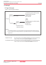
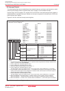
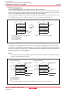
The CPU behavior during the interrupt sequence is described below. Figure 9.5 shows time required for
executing the interrupt sequence.
(1) The CPU obtains interrupt information (interrupt number and interrupt request level) by reading
address 000000h. Then, the IR bit applicable to the interrupt information is set to “0” (interrupt
requested).
(2) The FLG register, prior to an interrupt sequence, is saved to a temporary register
(1)
within the CPU.
(3) The I, D and U flags in the FLG register become as follows:
• The I flag is set to “0” (interrupt disabled)
• The D flag is set to “0” (single-step interrupt disabled)
• The U flag is set to “0” (ISP selected)
However, the U flag does not change state if an INT instruction for software interrupt Nos. 32 to 63 is
executed.
(4) The temporary register within the CPU is saved to the stack.
(5) The PC is saved to the stack.
(6) The interrupt priority level of the acknowledged interrupt in IPL is set.
(7) The start address of the relevant interrupt routine set in the interrupt vector is stored in the PC.
After the interrupt sequence is completed, an instruction is executed from the starting address of the
interrupt routine.
NOTE:
1. Temporary register cannot be modified by users.
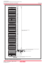
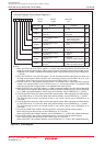
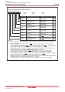
Figure 9.5 Time Required for Executing Interrupt Sequence
123456789 101112 13 14 15 16 17 18
SP-2
contents
SP-4
contents
vec
contents
vec+2
contents
Interrupt
information
Address
0000h
SP-2 SP-4 vec vec+2
PC
CPU clock
Address bus
Data bus
WR
(2)
RD
NOTES:
1. The indeterminate state depends on the instruction queue buffer.
A read cycle occurs when the instruction queue buffer is ready to accept instructions.
2. The WR signal timing shown here is for the case where the stack is located in the internal RAM.
Indeterminate
(1)
Indeterminate
(1)
Indeterminate
(1)