


Rev.1.10 Jul 01, 2005 page 33 of 318
REJ09B0124-0110
M16C/6N Group (M16C/6NK, M16C/6NM) 6. Processor Mode
Under development
This document is under development and its contents are subject to change.
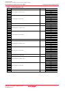
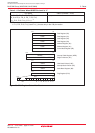
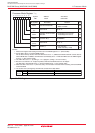
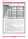
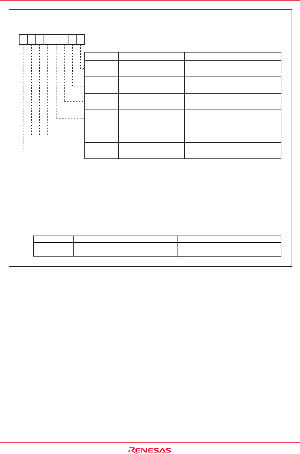
Figure 6.2 PM1 Register
Symbol Address After Reset
PM1 0005h 00001000b
PM17
PM13
PM12
PM10
-
(b1)
-
(b6-b4)
Data Block Enable Bit
(2)
Reserved Bit
Watchdog Timer Function
Select Bit
RW
RW
RW
RW
RW
RW
RW
0 : No wait state
1 : With wait state (1 wait)
Set to "0"
See NOTE 6
0 : Watchdog timer interrupt
1 : Watchdog timer reset
(3)
0 : Block A disable
1 : Block A enable
Set to "0"
NOTES:
1. Write to this register after setting the PRC1 bit in the PRCR register to "1" (write enable).
2. Set the PM10 bit to "0" for Mask ROM version.
For the flash memory version, when the PM10 bit is set to "1", addresses 0F000h to 0FFFFh can be used as
internal ROM area. In addition, the PM10 bit is automatically set to "1" while the FMR01 bit in the FMR0 register
is set to "1" (CPU rewrite mode).
3. The PM12 bit is set to "1" by writing a "1" in a program. (writing a "0" has no effect.)
4. Be sure to set this bit to "0" except for products with internal ROM area over 192 Kbytes.
The PM13 bit is automatically set to "1" when the FMR01 bit is "1" (CPU rewrite mode).
5. When the PM17 bit is set to "1" (with wait state), one wait state is inserted when accessing the internal RAM
or internal ROM.
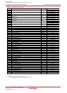
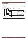
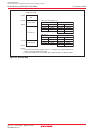
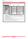
6. The access area is changed by the PM13 bit as listed in the table below.
Bit Name Function
Internal Reserved Area
Expansion Bit
(4)
Reserved Bit
Wait Bit
(5)
Processor Mode Register 1
(1)
000 0
Bit Symbol
b7 b6 b5 b4 b3 b2 b1 b0
Access area PM13 = 0 PM13 = 1
Internal
RAM
ROM
Up to addresses 00400h to 03FFFh (15 Kbytes)
Up to addresses D0000h to FFFFFh (192 Kbytes)
The entire are is usable
The entire are is usable