


Rev.1.10 Jul 01, 2005 page 169 of 318
REJ09B0124-0110
M16C/6N Group (M16C/6NK, M16C/6NM) 14. Serial I/O
Under development
This document is under development and its contents are subject to change.
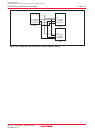
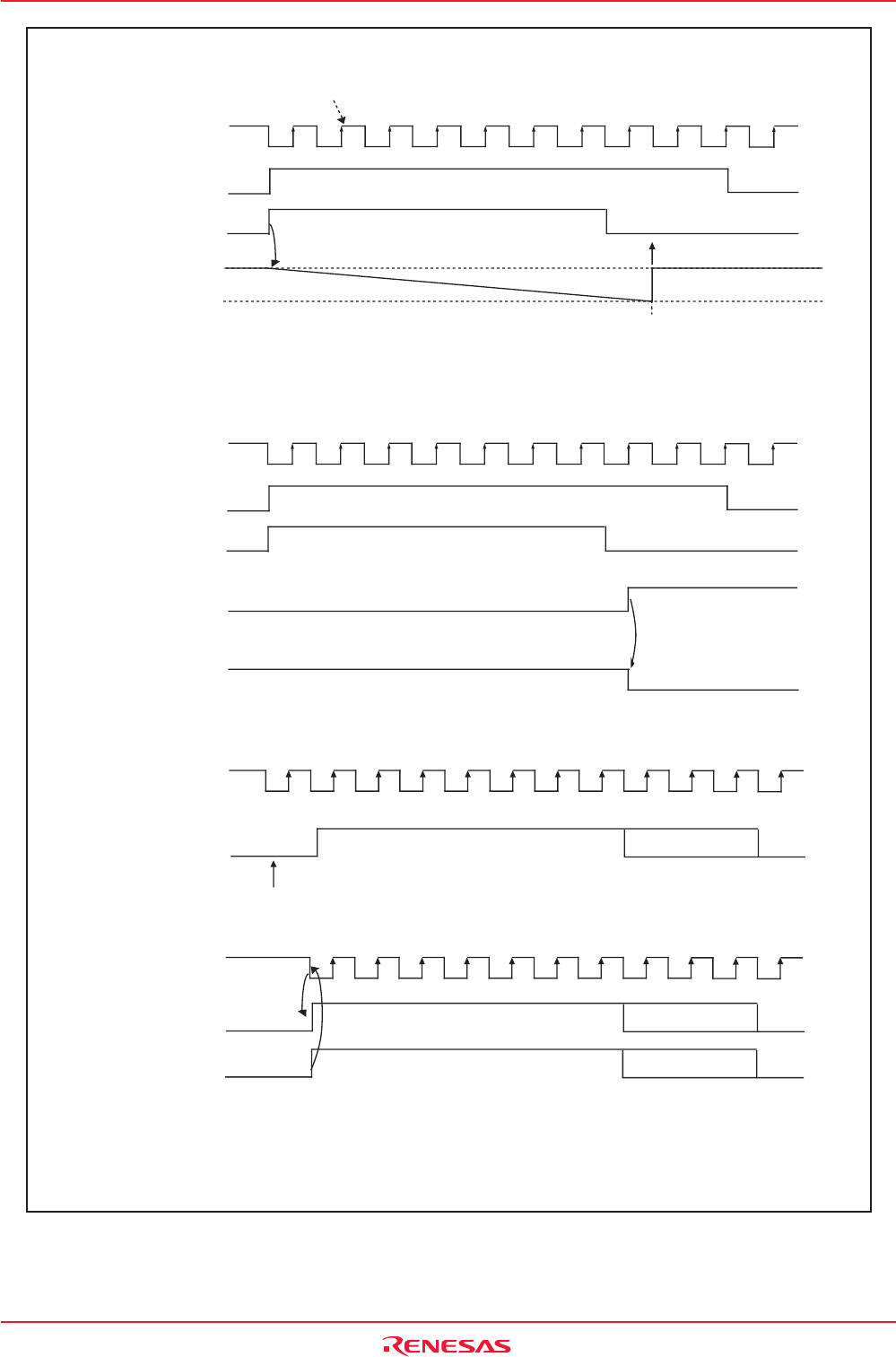
Figure 14.31 Bus Collision Detect Function-Related Bits
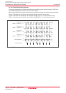
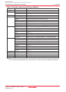
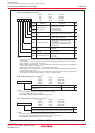
(3) SSS Bit in UiSMR Register (transmit start condition select)
Transmission enable condition is met
If SSS bit = 1, the serial I/O starts sending data at the rising edge
(1)
of RXDi
TXDi
CLKi
TXDi
RXDi
ST D0 D1 D2 D3 D4 D5 D6 D7 D8 SP
ST D0 D1 D2 D3 D4 D5 D6 D7 D8 SP
If SSS bit = 0, the serial I/O starts sending data one transfer clock cycle after the transmission enable condition is met.
Transfer clock
(NOTE 2)
NOTES:
1.The falling edge of RXDi when IOPOL bit = 0; the rising edge of RXDi when IOPOL bit = 1.
2.The transmit condition must be met before the falling edge
(1)
of RXDi.
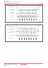
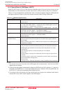
(2) ACSE Bit in UiSMR Register (auto clear of transmit enable bit)
TXDi
RXDi
ST D0 D1 D2 D3 D4 D5 D6 D7 D8 SP
Transfer clock
IR bit in
UiBCNIC register
TE bit in
UiC1 register
If the ACSE bit = 1 (automatically
clear when bus collision occurs),
the TE bit is set to "0"
(transmission disabled) when
the IR bit in the UiBCNIC register = 1
(unmatching detected).
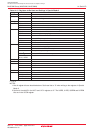
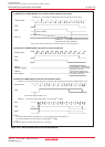
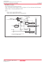
(1) ABSCS Bit in UiSMR Register (bus collision detect sampling clock select)
If ABSCS bit = 0, bus collision is determined at the rising edge of the transfer clock
Transfer clock
Timer Aj
TXDi
RXDi
ST D0 D1 D2 D3 D4 D5 D6 D7 D8 SP
Input to TAjIN
If ABSCS bit = 1, bus collision is determined when timer
Aj (one-shot timer mode) underflows.
Timer Aj: timer A3 when UART0; timer A4 when UART1; timer A0 when UART2
i = 0 to 2
This diagram applies to the case where IOPOL bit =1 (reversed)