


Rev.1.10 Jul 01, 2005 page 141 of 318
REJ09B0124-0110
M16C/6N Group (M16C/6NK, M16C/6NM) 14. Serial I/O
Under development
This document is under development and its contents are subject to change.
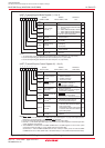
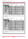
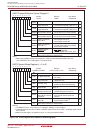
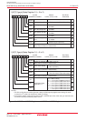
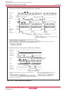
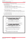
Figure 14.11 Transmit and Receive Operation
(1) Example of Transmit Timing (when internal clock is selected)
(2) Example of Receive Timing (when external clock is selected)
D0
D1
D2
D3
D4
D5
D6
D7
D0
D1
D2
D3
D4
D5
D6
D7
D0
D1
D2
D3
D4
D5
D6
D7
TC
TCLK
Stopped pulsing because the TE bit = 0
Write data to the UiTB register
TC = TCLK = 2(n + 1) / fj
fj: frequency of UiBRG count source (f1SIO, f2SIO, f8SIO, f32SIO)
n: value set to the UiBRG register
i = 0 to 2
Transfer clock
TE bit in
UiC1 register
TI bit in
UiC1 register
CLKi
TXDi
"H"
"L"
"0"
"1"
"0"
"1"
"0"
"1"
CTSi
"0"
"1"
Stopped pulsing because CTSi = H
1 / f
EXT
Write dummy data to the UiTB register
TE bit in
UiC1 register
TI bit in
UiC1 register
CLKi
RXDi
RI bit in
UiC1 register
RTSi
"H"
"L"
"0"
"1"
"0"
"1"
"0"
"1"
RE bit in
UiC1 register
"0"
"1"
Receive data is taken in
Transferred from the UiTB register to the UARTi transmit register
Read out from the UiRB register
fEXT: frequency of external clock
Transferred from UARTi receive register
to the UiRB register
IR bit in
SiRIC register
"0"
"1"
D0
D1
D2
D3
D4
D5
D6
D7
D0
D1
D2
D3
D4
D5
Transferred from the UiTB register to the UARTi transmit register
Make sure the following conditions are met when input
to the CLKi pin before receiving data is high:
TE bit in UiC1 register = 1 (transmission enabled)
RE bit in UiC1 register = 1 (reception enabled)
Write dummy data to the UiTB register
The above timing diagram applies to the case where the register bits are set as follows:
CKDIR bit in UiMR register = 0 (internal clock)
CRD bit in UiC0 register = 0 (CTS/RTS enabled), CRS bit in UiC0 register = 0 (CTS selected)
CKPOL bit in UiC0 register = 0 (transmit data output at the falling edge and receive data taken in at the rising edge of the transfer clock)
UiRS bit = 0 (an interrupt request occurs when the transmit buffer becomes empty):
U0IRS bit is bit 0 in UCON register
U1IRS bit is bit 1 in UCON register
U2IRS bit is bit 4 in U2C1 register
Set to "0" when interrupt request is
accepted, or set to "0" in a program
Set to "0" when interrupt request is accepted, or set to "0" in a program
The above timing diagram applies to the case where the register bits are set
as follows:
CKDIR bit in UiMR register = 1 (external clock)
CRD bit in UiC0 register = 0 (CTS/RTS enabled), CRS bit = 1 (RTS selected)
CKPOL bit in UiC0 register = 0 (transmit data output at the falling edge and receive
data taken in at the rising edge of the transfer clock)
TXEPT bit in
UiC0 register
IR bit in
SiTIC register
Even if the reception is completed, the RTS
does not change. The RTS becomes "L"
when the RI bit changes to "0" from "1".