


Rev.1.10 Jul 01, 2005 page 275 of 318
REJ09B0124-0110
M16C/6N Group (M16C/6NK, M16C/6NM) 21. Electric Characteristics
Under development
This document is under development and its contents are subject to change.
2
150
150
ms
µs
µs
Time for Internal Power Supply Stabilization During Powering-On
STOP Release Time
Low Power Dissipation Mode Wait Mode Release Time
td(P-R)
td(R-S)
td(W-S)
Symbol
Parameter
Min.
Standard
Unit
Measuring
Condition
Max.
Typ.
VCC = 3.0 to 5.5V
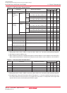
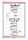
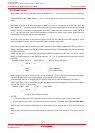
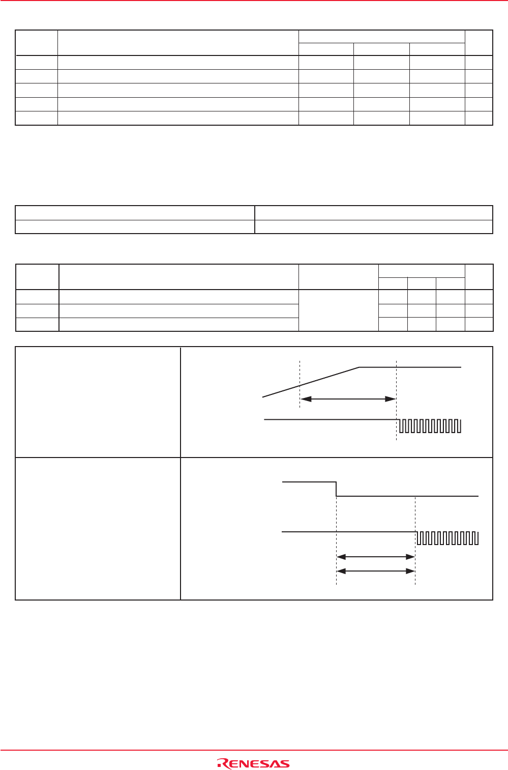
Table 21.10 Power Supply Circuit Timing Characteristics
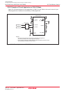
CPU clock
VCC
t
d(P-R)
td(P-R)
Time for Internal Power Supply
Stabilization During Powering-On
t
d(R-S)
STOP Release Time
t
d(W-S)
Low Power Dissipation Mode
Wait Mode Release Time
CPU clock
td(W-S)
td(R-S)
(b)
(a)
Interrupt for
(a) Stop mode release
or
(b) Wait mode release
Figure 21.2 Power Supply Circuit Timing Diagram
NOTES:
1. Referenced to VCC = 4.5 to 5.5V, 3.0 to 3.6V, Topr = 0 to 60°C unless otherwise specified.
2. n denotes the number of blocks to erase.
Table 21.9 Flash Memory Version Program/Erase Voltage and Read Operation Voltage Characteristics
(at Topr = 0 to 60°C)
200
4
4 ✕ n
(2)
200
15
µs
s
s
µs
µs
Word Program Time
Block Erase Time
Erase All Unlocked Blocks Time
Lock Bit Program Time
Flash Memory Circuit Stabilization Wait Time
Parameter
Min.
Standard
Unit
Max.Typ.
30
1
1 ✕ n
(2)
30
Symbol
-
-
-
-
tps
VCC = 3.3 ± 0.3V or 5.0 ± 0.5V
Flash Read Operation VoltageFlash Program, Erase Voltage
VCC = 3.0 to 5.5V
Table 21.8 Flash Memory Version Electrical Characteristics
(1)