


Rev.1.10 Jul 01, 2005 page 31 of 318
REJ09B0124-0110
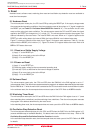
M16C/6N Group (M16C/6NK, M16C/6NM) 5. Reset
Under development
This document is under development and its contents are subject to change.
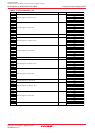
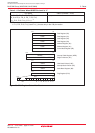
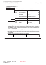
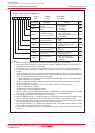
P0, P1, P2, P3, P4, P5, P6, P7, Input port
P8_0 to P8_4, P8_6, P8_7, P9, P10,
P11, P12, P13, P14_0, P14_1
(2)
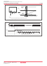
____________
Table 5.1 Pin Status When RESET Pin Level is “L”
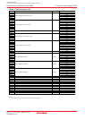
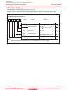
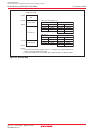
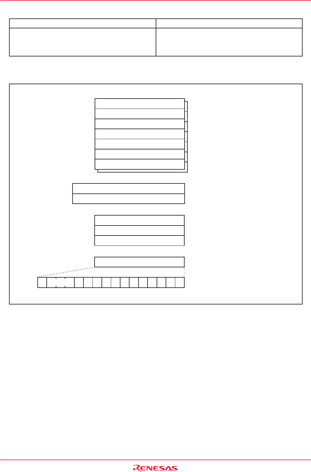
Figure 5.3 CPU Register Status After Reset
0000h
0000h
0000h
b15 b0
Static Base Register (SB)
User Stack Pointer (USP)
Interrupt Stack Pointer (ISP)
b19
00000h
b0
Interrupt Table Register (INTB)
Content of addresses FFFFEh to FFFFCh
Program Counter (PC)
b15 b0
0000h
0000h
0000h
0000h
0000h
0000h
0000h
Data Register (R0)
Data Register (R1)
Data Register (R2)
Data Register (R3)
Address Register (A0)
Address Register (A1)
Frame Base Register (FB)
b15 b0
b15 b0
0000h
Flag Register (FLG)
IPL U I O B S Z D C
b7b8
Pin Name Status (CNVSS = VSS)
NOTE:
1. P11, P12, P13, P14_0 and P14_1 pins are only in the 128-pin version.