


Rev.1.10 Jul 01, 2005 page 181 of 318
REJ09B0124-0110
M16C/6N Group (M16C/6NK, M16C/6NM) 15. A/D Converter
Under development
This document is under development and its contents are subject to change.
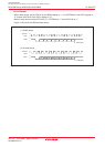
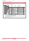
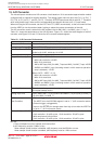
Item Performance
Method of A/D Conversion Successive approximation (capacitive coupling amplifier)
Analog Input Voltage
(1)
0V to AVCC (VCC)
Operating Clock φAD
(2)
fAD, divide-by-2 of fAD, divide-by-3 of fAD, divide-by-4 of fAD,
divide-by-6 of fAD, divide-by-12 of fAD
Resolution 8 bits or 10 bits (selectable)
Integral Nonlinearity Error When AVCC = VREF = 5 V
• With 8-bit resolution: ±2LSB
• With 10-bit resolution
AN0 to AN7 input, AN0_0 to AN0_7 input and AN2_0 to AN2_7 input: ±3LSB
ANEX0 and ANEX1 input (including mode in which external operation
amp is selected): ±7LSB
When AVCC = VREF = 3.3 V
• With 8-bit resolution: ±2LSB
• With 10-bit resolution
AN0 to AN7 input, AN0_0 to AN0_7 input and AN2_0 to AN2_7 input: ±5LSB
ANEX0 and ANEX1 input (including mode in which external operation
amp is selected): ±7LSB
Operating Modes One-shot mode, repeat mode, single sweep mode, repeat sweep mode 0,
and repeat sweep mode 1
Analog Input Pins 8 pins (AN0 to AN7) + 2 pins (ANEX0 and ANEX1) + 8 pins (AN0_0 to AN0_7)
+ 8 pins (AN2_0 to AN2_7)
A/D Conversion • Software trigger
Start Condition The ADST bit in the ADCON0 register is set to “1” (A/D conversion starts)
• External trigger (retriggerable)
_____________
Input on the ADTRG pin changes state from high to low after the ADST bit
is set to “1” (A/D conversion starts)
Conversion Speed Per Pin • Without sample and hold function
8-bit resolution: 49 φAD cycles, 10-bit resolution: 59 φAD cycles
• With sample and hold function
8-bit resolution: 28 φAD cycles, 10-bit resolution: 33 φAD cycles
NOTES:
1. Does not depend on use of sample and hold function.
2. φAD frequency must be 10 MHz or less.
When sample & hold function is disabled, φAD frequency must be 250 kHz or more.
When sample & hold function is enabled, φAD frequency must be 1 MHz or more.
15. A/D Converter
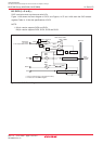
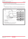
The microcomputer contains one A/D converter circuit based on 10-bit successive approximation method
configured with a capacitive-coupling amplifier. The analog inputs share the pins with P10_0 to P10_7,
_____________
P9_5, P9_6, P0_0 to P0_7, and P2_0 to P2_7. Similarly, ADTRG input shares the pin with P9_7. Therefore,
when using these inputs, make sure the corresponding port direction bits are set to “0” (input mode).
When not using the A/D converter, set the VCUT bit to “0” (VREF unconnected), so that no current will flow
from the VREF pin into the resistor ladder, helping to reduce the power consumption of the chip.
The A/D conversion result is stored in the ADi register’s bits for ANi, AN0_i, and AN2_i pins (i = 0 to 7).
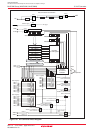
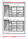
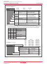
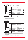
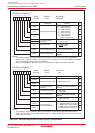
Table 15.1 shows the performance of the A/D converter. Figure 15.1 shows the block diagram of the A/D
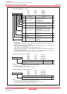
converter, and Figures 15.2 and 15.3 show the A/D converter-related registers.
Table 15.1 A/D Converter Performance