


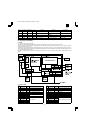
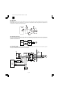
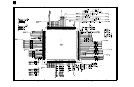

(8) Toner supply motor drive circuit
The IC31 is the motor control IC, which generates the pseudo AC waveform with the pulse signals (TM, TM-) outputted from ASIC, driving the toner
supply motor.
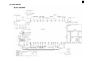
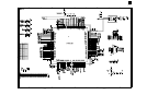
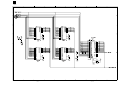
3. CCD PWB
The CCD PWB is provided with the CCD (Charge-Coupled Device), the differential amplifier which amplifies image signals, and the AD convertor
which converts the amplified image signals into digital signals.
The DC power and the pulse supply pins necessary for operating the CCD image sensor are the power source (CD pin), GND (SS pin), shift pulse
(SH pin), transfer pulse (φ 1 pin), (φ 2 pin), reset pulse (/RS pin), clamp pulse (/CP pin), and sampling (/SP pin).
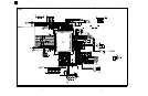
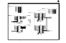
Photo data are stored in the light receiving element at the center of the CCD by the SH signal. Even number pixel data are sent to one of the two
shift registers which are positioned at both ends of the light receiving element, and odd number pixel data are sent to the other shift register. The
time interval between inputting two SH signals is called the photo accumulation time.
The signals are transfered to the register, then to the shift register sequentially by transfer pulses φ 1 and φ 2 and to the floating capacitor section
where electric signals are voltage-converted. Electric charges from the even number pixel shift register and the odd number pixel shift register are
flowed to the floating capacitor section alternatively.
The /RS signal is the reset signal of the CCD output signal. The CCD output is expressed as electric charges equivalently accumulated in the
capacitor. Therefore, to take the CCD output data one pixel by one pixel, one output data must be cleared after it is outputted. The /RS signal is
used for that operation.
The /SP pulse signal is the peak hold signal of the signal voltage.
The output signal from the CCD is amplified by about 4.7 times greater in the differential amplifier circuit in the CCD PWB.
Differential amplification is made for the signal output (OS) and the compensation output (DOS).
The amplified CCD signal output is sent to the clamp circuit. In the clamp circuit, the black level is clamped to 2V at the BCLK signal timing by the
analog switch. The clamped voltage is maintained for one line by the coupling capacitor. The clamped analog signal is impedance-converted and
inputted to the AD convertor.
The analog signal inputted to the AD convertor is converted into 8bit digital data and passed to the PCU PWB.
The machine employs the TCD1501C as the image sensor. The TCD1501C is the reduction type high sensitivity CCD linear sensor of one-output
system. 5000 pixels of 7um x 7um are arranged in line to allow scanning of A3 document at 400dpi (16 lines/mm).
AR-161
AR-160/161 FM/E [13] ELECTRICAL SECTION 12/1/1998
13 – 13