www.ti.com
Peripheral Architecture
2 Peripheral Architecture
The DDR2 memory controller can gluelessly interface to most standard DDR2 SDRAM devices and
supports such features as self-refresh mode and prioritized refresh. In addition, it provides flexibility
through programmable parameters such as the refresh rate, CAS latency, and many SDRAM timing
parameters.
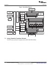
The following sections describe the architecture of the DDR2 memory controller as well as how to
interface and configure it to perform read and write operations to DDR2 SDRAM devices. Also, Section 3
provides a detailed example of interfacing the DDR2 memory controller to a common DDR2 SDRAM
device.
2.1 Clock Control
The DDR2 memory controller is clocked directly from the output of the second phase-locked loop (PLL2)
of C6455/C6454 devices. The PLL2 multiplies its input clock by 20. This clock is divided by 2 to generate
DDR2CLKOUT. The frequency of DDR2CLKOUT can be determined by using the following formula:
DDR2CLKOUT frequency = (PLL2 input clock frequency × 20)/2 = PLL2 input clock frequency×10
The second output clock of the DDR2 memory controller, DDR2CLKOUT, is the inverse of
DDR2CLKOUT. For more information on the PLL2, see the device-specific data manual.
2.2 Memory Map
For information describing the device memory map, see the device-specific data manual.
2.3 Signal Descriptions
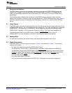
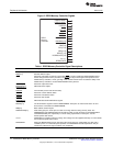
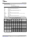
The DDR2 memory controller signals are shown in Figure 2 and described in Table 1. The following
features are included:
• The maximum width for the data bus (DED[31:0]) is 32-bits.
• The address bus (DEA[13:0]) is 14-bits wide with an additional 3 bank address pins (DBA[2:0]).
• Two differential output clocks (DDR2CLKOUT and DDR2CLKOUT) driven by internal clock sources.
• Command signals: Row and column address strobe (DSDRAS and DSDCAS), write enable strobe
(DSDWE), data strobe (DSDDQS[3:0] and DSDDQS[3:0]), and data mask (DSDDQM[3:0]).
• One chip select signal (DCE0).
• One clock enable signal (DSDCKE).
• Two on-die termination output signals (DEODT[1:0]). (These pins are reserved for future use.)
11
SPRU970G–December 2005–Revised June 2011 C6455/C6454 DDR2 Memory Controller
Submit Documentation Feedback
Copyright © 2005–2011, Texas Instruments Incorporated


