www.ti.com
Peripheral Architecture
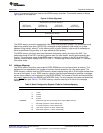
• Following a write to the two least-significant bytes in the SDRAM configuration register (SDCFG); see
Section 2.11.3.
At the end of the initialization sequence, the DDR2 memory controller performs an auto-refresh cycle,
leaving the DDR2 memory controller in an idle state with all banks deactivated.
When the initialization section is started automatically after a hard or soft reset, commands and data
stored in the DDR2 memory controller FIFOs are lost. However, when the initialization sequence is
initiated by a write to the two least-significant bytes in SDCFG, data and commands stored in the DDR2
memory controller FIFOs are not lost and the DDR2 memory controller ensures read and write commands
are completed before starting the initialization sequence.
2.11.1 DDR2 SDRAM Device Mode Register Configuration Values
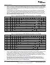
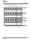
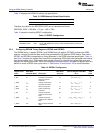
The DDR2 memory controller initializes the mode register and extended mode register 1 of the memory
device with the values shown on Table 9 and Table 10. The DDR2 SDRAM extended mode registers 2
and 3 are configured with a value of 0h.
Table 9. DDR2 SDRAM Mode Register Configuration
Mode
Register Bit Mode Register Field Init Value Description
12 Power-down Mode 0 Active power-down exit time bit. Configured for Fast exit.
11-9 Write Recovery SDTIM1.T_WR Write recovery bits for auto-precharge. Initialized using
the T_WR bits of the SDRAM timing 1 register (SDTIM1).
8 DLL Reset 0 DLL reset bits. DLL is not in reset.
7 Mode 0 Operating mode bit. Normal operating mode is always
selected.
6-4 CAS Latency SDCFG.CL CAS latency bits. Initialized using the CL bits of the
SDRAM configuration register (SDCFG).
3 Burst Type 0 Burst type bits. Sequential burst mode is always used.
2-0 Burst Length 3h Bust length bits. A burst length of 8 is always used.
Table 10. DDR2 SDRAM Extended Mode Register 1 Configuration
Mode
Register Bit Mode Register Field Init Value Description
12 Output Buffer Enable 0 Output buffer enable bits. Output buffer is always
enabled.
11 RDQS Enable 0 RDQS enable bits. Always initialized to 0 (RDQS signals
disabled.)
10 DQS enable 0 DQS enable bit. Always initialized to 0 (DQS signals
enabled.)
9-7 OCD Operation 0h Off-chip driver impedance calibration bits. This bit is
always initialized to 0h.
6 ODT Value (Rtt) 0 On-die termination effective resistance (Rtt) bit. This bit is
reserved for future use.
5-3 Additive Latency 0h Additive latency bits. Always initialized to 0h (no additive
latency).
2 ODT Value (Rtt) 1 On-die termination effective resistance (Rtt) bit. This bit is
reserved for future use.
1 Output Driver Impedance SDCFG.DDR_DRIVE Output driver impedance control bits. Initialized using the
DDR_DRIVE bit of the SDRAM configuration register
(SDCFG).
0 DLL Enable 0 DLL enable/disable bits. DLL is always enabled.
29
SPRU970G–December 2005–Revised June 2011 C6455/C6454 DDR2 Memory Controller
Submit Documentation Feedback
Copyright © 2005–2011, Texas Instruments Incorporated


