


Contents
Preface ....................................................................................................................................... 7
1 Introduction ........................................................................................................................ 9
1.1 Purpose of the Peripheral .............................................................................................. 9
1.2 Features .................................................................................................................. 9
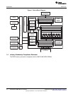
1.3 Functional Block Diagram .............................................................................................. 9
1.4 Industry Standard(s) Compliance Statement ....................................................................... 10
2 Peripheral Architecture ...................................................................................................... 11
2.1 Clock Control ........................................................................................................... 11
2.2 Memory Map ............................................................................................................ 11
2.3 Signal Descriptions .................................................................................................... 11
2.4 Protocol Description(s) ................................................................................................ 13
2.5 Memory Width, Byte Alignment, and Endianness ................................................................. 20
2.6 Address Mapping ...................................................................................................... 21
2.7 DDR2 Memory Controller Interface .................................................................................. 24
2.8 Refresh Scheduling .................................................................................................... 27
2.9 Self-Refresh Mode ..................................................................................................... 28
2.10 Reset Considerations .................................................................................................. 28
2.11 DDR2 SDRAM Memory Initialization ................................................................................ 28
2.12 Interrupt Support ....................................................................................................... 30
2.13 EDMA Event Support .................................................................................................. 30
2.14 Emulation Considerations ............................................................................................. 30
3 Using the DDR2 Memory Controller ..................................................................................... 31
3.1 Connecting the DDR2 Memory Controller to DDR2 SDRAM .................................................... 31
3.2 Configuring DDR2 Memory Controller Registers to Meet DDR2 SDRAM Specifications .................... 35
4 DDR2 Memory Controller Registers ..................................................................................... 38
4.1 Module ID and Revision Register (MIDR) .......................................................................... 39
4.2 DDR2 Memory Controller Status Register (DMCSTAT) .......................................................... 40
4.3 SDRAM Configuration Register (SDCFG) .......................................................................... 41
4.4 SDRAM Refresh Control Register (SDRFC) ....................................................................... 43
4.5 SDRAM Timing 1 Register (SDTIM1) ............................................................................... 44
4.6 SDRAM Timing 2 Register (SDTIM2) ............................................................................... 46
4.7 Burst Priority Register (BPRIO) ...................................................................................... 47
4.8 DDR2 Memory Controller Control Register (DMCCTL) ........................................................... 48
Revision History ......................................................................................................................... 49
3
SPRU970G–December 2005–Revised June 2011 Table of Contents
Submit Documentation Feedback
Copyright © 2005–2011, Texas Instruments Incorporated