0 1 2 3 MBank 0
Row 0
Row 1
Row 2
Row N
C
o
l l
C
o
l
C
o
l
C
o
Row 0
Row N
Row 1
Row 2
CC
Bank 1
l l
0 21
oo
C C
l l
3
M
o o
Row 0
Row N
Row 1
Row 2
CC
Bank 2
l l
0 21
oo
llll
Row N
Row 2
Row 0
Row 1
Bank P 0 1 2 3 M
C C
l l
3 M
o o
o
C
o
C
o
C
o
C
Peripheral Architecture
www.ti.com
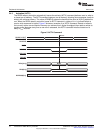
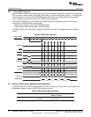
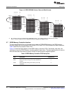
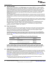
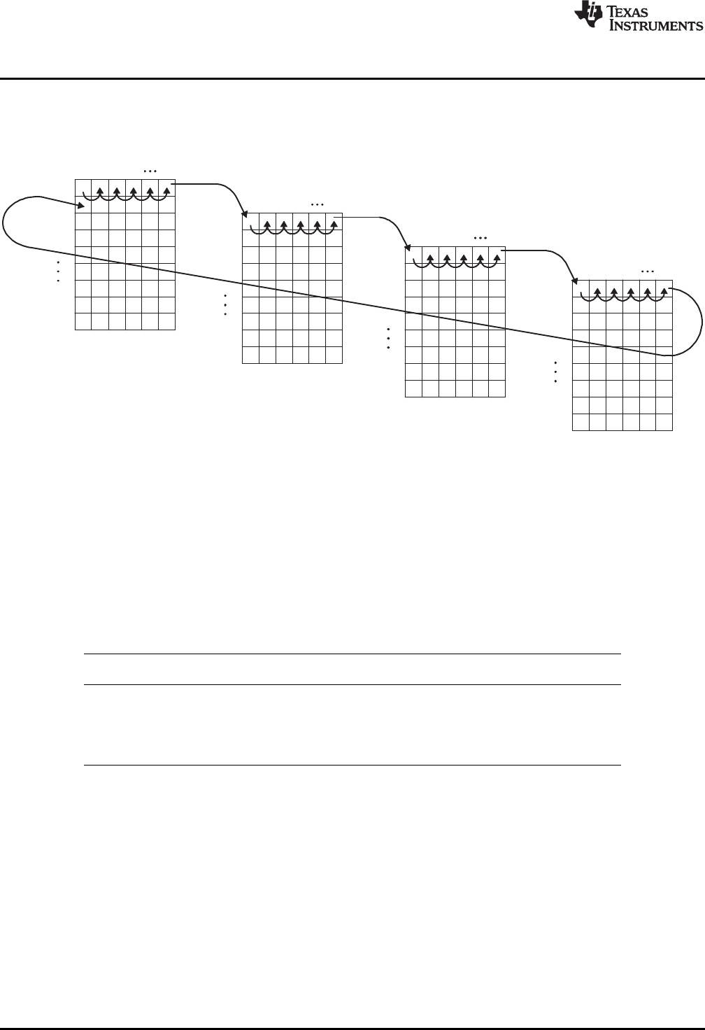
Figure 14. DDR2 SDRAM Column, Row, and Bank Access
A M is number of columns (as determined by PAGESIZE) minus 1, P is number of banks (as determined by IBANK)
minus 1, and N is number of rows (as determined by both PAGESIZE and IBANK) minus 1.
2.7 DDR2 Memory Controller Interface
To move data efficiently from on-chip resources to external DDR2 SDRAM device, the DDR2 memory
controller makes use of a command FIFO, a write FIFO, a read FIFO, and command and data schedulers.
Table 6 describes the purpose of each FIFO.
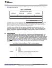
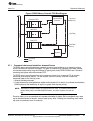
Figure 15 shows the block diagram of the DDR2 memory controller FIFOs. Commands, write data, and
read data arrive at the DDR2 memory controller parallel to each other. The same peripheral bus is used to
write and read data from external memory as well as internal memory-mapped registers.
Table 6. DDR2 Memory Controller FIFO Description
Depth (64-Bit
FIFO Description Doublewords)
Command Stores all commands coming from on-chip requestors 7
Write Stores write data coming from on-chip requestors to 11
memory
Read Stores read data coming from memory to on-chip 17
requestors
24
C6455/C6454 DDR2 Memory Controller SPRU970G–December 2005–Revised June 2011
Submit Documentation Feedback
Copyright © 2005–2011, Texas Instruments Incorporated


