


www.ti.com
DDR2 Memory Controller Registers
4.3 SDRAM Configuration Register (SDCFG)
The SDRAM configuration register (SDCFG) contains fields that program the DDR2 memory controller to
meet the specification of the DDR2 memory. These fields configure the DDR2 memory controller to match
the data bus width, CAS latency, number of internal banks, and page size of the external DDR2 memory.
Bits 0-14 of the SDCFG register are only writeable when the TIMUNLOCK bit is set to 0 (unlocked). for
more information on initializing the configuration registers of the DDR2 memory controller, see
Section 2.11.1. The SDCFG register is shown in Figure 21 and described in Table 20.
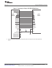
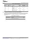
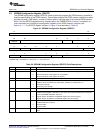
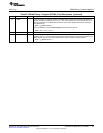
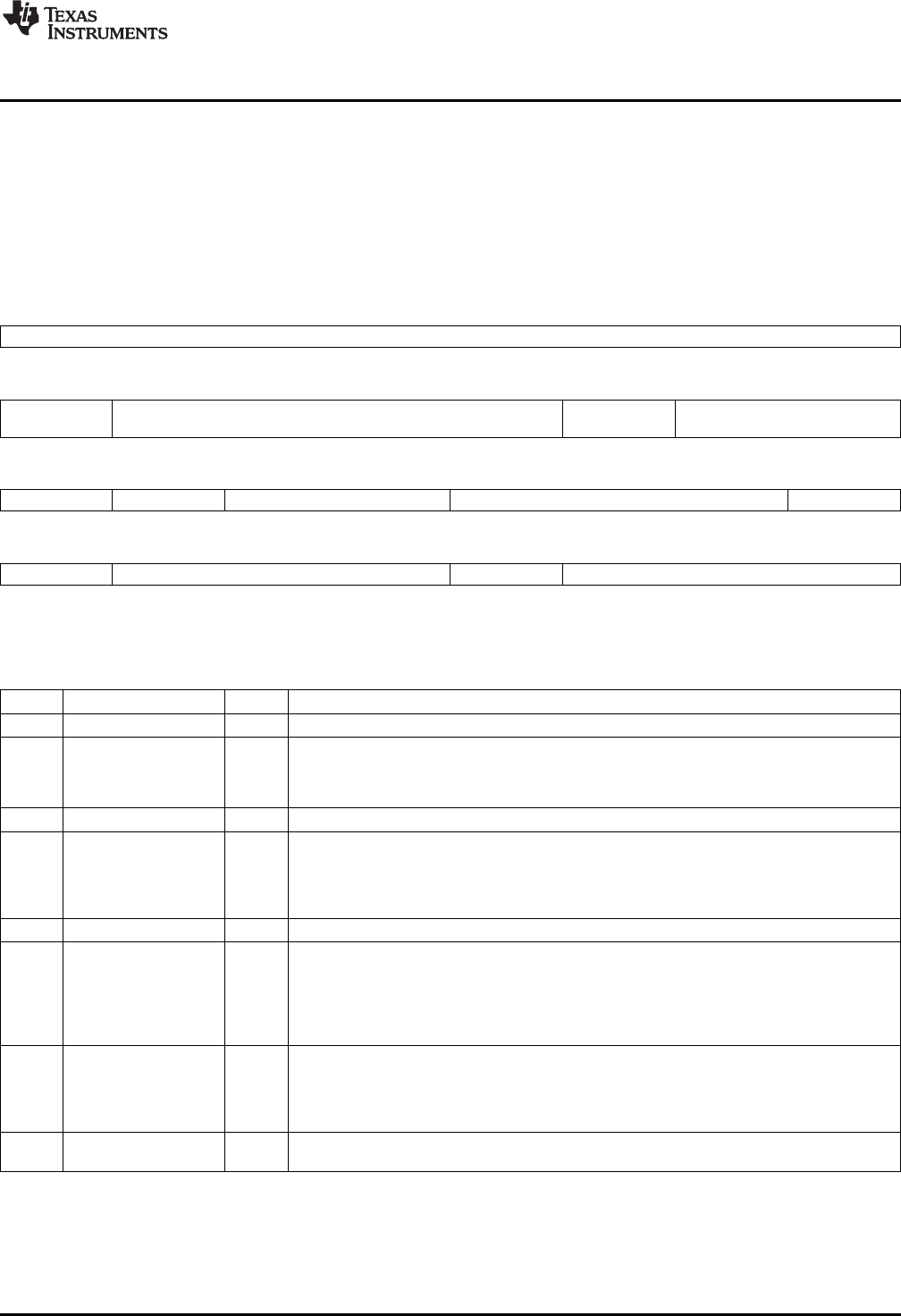
Figure 21. SDRAM Configuration Register (SDCFG)
31 24
Reserved
R-0x0
23 22 19 18 17 16
BOOT_
Reserved DDR_DRIVE Reserved
UNLOCK
R/W-0 R/W-0xA R-0 R-0x3
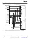
15 14 13 12 11 9 8
TIMUNLOCK NM Reserved CL Reserved
R/W-0 R/W-0 R-0x0 R/W-0x5 R-0x0
7 6 4 3 2 0
Reserved IBANK Reserved PAGESIZE
R-0x0 R/W-0x2 R-0x0 R/W-0x0
LEGEND: R/W = Read/Write; R = Read only; -n = value after reset
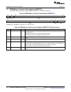
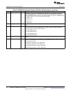
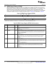
Table 20. SDRAM Configuration Register (SDCFG) Field Descriptions
Bit Field Value Description
31-24 Reserved Reserved. Writes to this register must keep these bits at their default values.
23 BOOT_UNLOCK Boot unlock bit. Controls write access to bits 16-22 and 27 of this register.
0 Writes to bits 22:16 of this register are not permitted.
1 Writes to bits 22:16 of this register are allowed.
22-19 Reserved Reserved. Writes to this register must keep these bits at their default value.
18 DDR_DRIVE DDR2 SDRAM drive strength. This bit is used to select the drive strength used by the DDR2
SDRAM. This bit is writeable only when BOOT_UNLOCK is unlocked (set to 1).
0 Normal drive strength.
1 Weak (60%) drive strength.
17-16 Reserved Reserved. Writes to this register must keep these bits at their default value.
15 TIMUNLOCK Timing unlock bit. Controls write access for the SDRAM Timing Register (SDTIM1) and
SDRAM Timing Register 2 (SDTIM2). A write to this bit causes the DDR2 Memory Controller
to start the SDRAM initialization sequence.
0 Register fields in the SDTIM1 and SDTIM2 registers may not be changed.
1 Register fields in the SDTIM1 and SDTIM2 registers may be changed.
14 NM DDR2 data bus width. A write to this bit will cause the DDR2 Memory Controller to start the
SDRAM initialization sequence.
0 32-bit bus width.
1 16-bit bus width
13-12 Reserved Reserved. The reserved bit location is always read as 0. A value written to this field has no
effect.
41
SPRU970G–December 2005–Revised June 2011 C6455/C6454 DDR2 Memory Controller
Submit Documentation Feedback
Copyright © 2005–2011, Texas Instruments Incorporated