


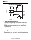
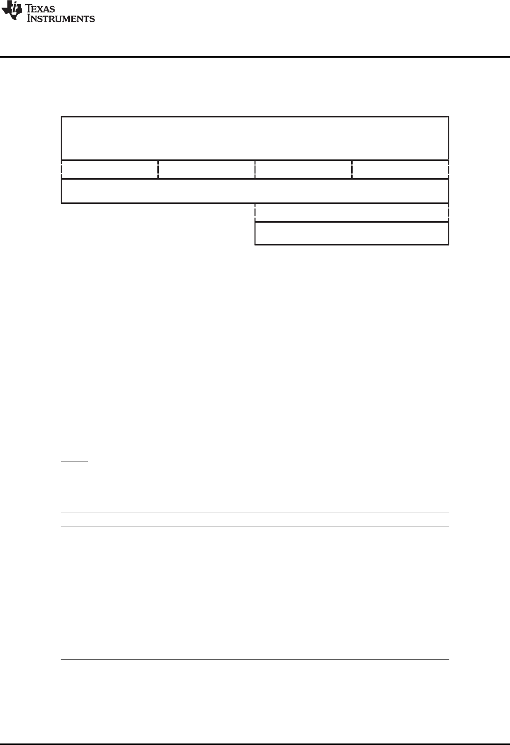
DDR2 memory controller data bus
DED[31:24]
(Byte Lane 3)
DED[23:16]
(Byte Lane 2)
DED[15:8]
(Byte Lane 1)
DED[7:0]
(Byte Lane 0)
32-bit memory device
16-bit memory device
www.ti.com
Peripheral Architecture
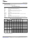
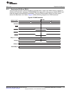
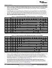
Figure 10 shows the byte lanes used on the DDR2 memory controller. The external memory is always
right aligned on the data bus.
Figure 10. Byte Alignment
The DDR2 memory controller supports both little endian and big endian formats. The endianness mode
determines whether byte lane 0 (DED[7:0]) is accessed as byte address 0 (little endian) or as byte
address N (big endian), where 2
n
is the memory width in bytes. Similarly, byte lane N is addresses as
either byte address 0 (big endian) or as byte address N (little endian).
The DDR2 memory controller uses the endianness mode being used by the rest of the DSP. The
endianness mode of the DSP is set during device reset (for more details, see the device-specific data
manual. The endianness mode of the DDR2 memory controller is shown on the BE bit of the DDR2
memory controller status register (DMCSTAT); BE = 1 indicates big endian mode and BE = 0 indicates
little endian mode.
2.6 Address Mapping
The DDR2 memory controller views external DDR2 SDRAM as one continuous block of memory. This
statement is true regardless of the number of memory devices located on the chip select space. The
DDR2 memory controller receives DDR2 memory access requests along with a 32-bit logical address from
the rest of the system. In turn, DDR2 memory controller uses the logical address to generate a row/page,
column, bank address, and chip selects for the DDR2 SDRAM. The number of column and bank address
bits used is determined by the IBANK and PAGESIZE fields. The chip selection pins used are determined
by the DCE0 field (see Table 5). The DDR2 memory controller uses up to 14 bits for the row/page
address.
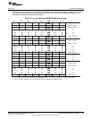
Table 5. Bank Configuration Register Fields for Address Mapping
Bit Field Bit Value Bit Description
IBANK Defines the number of internal banks on the external DDR2 memory.
0 1 bank
1h 2 banks
2h 4 banks
3h 8 banks
PAGESIZE Defines the page size of each page of the external DDR2 memory.
0 256 words (requires 8 column address bits)
1h 512 words (requires 9 column address bits)
2h 1024 words (requires 10 column address bits)
3h 2048 words (requires 11 column address bits)
21
SPRU970G–December 2005–Revised June 2011 C6455/C6454 DDR2 Memory Controller
Submit Documentation Feedback
Copyright © 2005–2011, Texas Instruments Incorporated