


DED[31:0]
DSDDQS[3:0]
COL
BANK
DEA[10]
CASLatency
D0
D1 D2
D3
D4
D5
D6
D7
DDR2CLKOUT
DDR2CLKOUT
DCE0
DSDCKE
DSDRAS
DSDWE
DSDDQM[3:0]
DSDCAS
DBA[2:0]
DEA[13:0]
www.ti.com
Peripheral Architecture
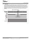
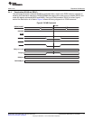
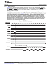
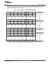
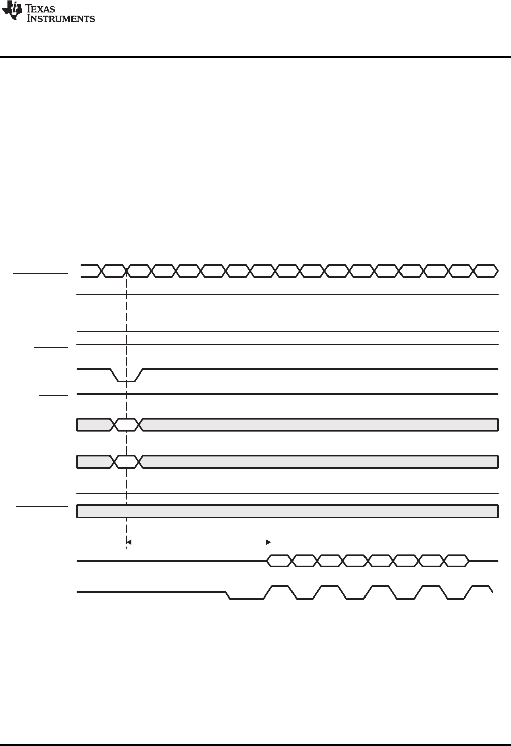
2.4.5 READ Command
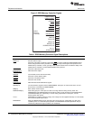
Figure 8 shows the DDR2 memory controller performing a read burst from DDR2 SDRAM. The READ
command initiates a burst read operation to an active row. During the READ command, DSDCAS drives
low, DSDWE and DSDRAS remain high, the column address is driven on DEA[12:0], and the bank
address is driven on DBA[2:0].
The DDR2 memory controller uses a burst length of 8, and has a programmable CAS latency of 2, 3, 4, or
5. The CAS latency is three cycles in Figure 8. Read latency is equal to CAS latency plus additive latency.
The DDR2 memory controller always configures the memory to have an additive latency of 0, so read
latency equals CAS latency. Since the default burst size is 8, the DDR2 memory controller returns 8
pieces of data for every read command. If additional accesses are not pending to the DDR2 memory
controller, the read burst completes and the unneeded data is disregarded. If additional accesses are
pending, depending on the scheduling result, the DDR2 memory controller can terminate the read burst
and start a new read burst. Furthermore, the DDR2 memory controller does not issue a DCAB/DEAC
command until page information becomes invalid.
Figure 8. DDR2 READ Command
19
SPRU970G–December 2005–Revised June 2011 C6455/C6454 DDR2 Memory Controller
Submit Documentation Feedback
Copyright © 2005–2011, Texas Instruments Incorporated