www.ti.com
Peripheral Architecture
2.4 Protocol Description(s)
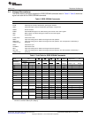
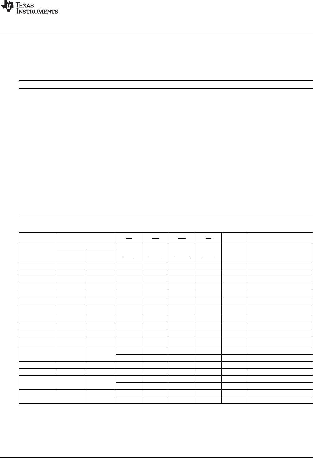
The DDR2 memory controller supports the DDR2 SDRAM commands listed in Table 2. Table 3 shows the
signal truth table for the DDR2 SDRAM commands.
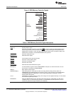
Table 2. DDR2 SDRAM Commands
Command Function
ACTV Activates the selected bank and row.
DCAB Precharge all command. Deactivates (precharges) all banks.
DEAC Precharge single command. Deactivates (precharges) a single bank.
DESEL Device Deselect.
EMRS Extended Mode Register set. Allows altering the contents of the mode register.
MRS Mode register set. Allows altering the contents of the mode register.
NOP No operation.
Power Down Power down mode.
READ Inputs the starting column address and begins the read operation.
READ with Inputs the starting column address and begins the read operation. The read operation is followed by a
autoprecharge precharge.
REFR Autorefresh cycle.
SLFREFR Self-refresh mode.
WRT Inputs the starting column address and begins the write operation.
WRT with Inputs the starting column address and begins the write operation. The write operation is followed by a
autoprecharge precharge.
Table 3. Truth Table for DDR2 SDRAM Commands
DDR2 SDRAM
Signals CKE CS RAS CAS WE BA[2:0] A[13:11, 9:0] A10
DSDCKE
DDR2 Memory Previous
Controller Signals Cycles Current Cycle DCE0 DSDRAS DSDCAS DSDWE DBA[2:0] DEA[13:11, 9:0] DEA[10]
ACTV H
(1)
H L L H H Bank Row Address
DCAB H H L L H L X X H
DEAC H H L L H L Bank X L
MRS H H L L L L BA
(2)
OP Code
EMRS H H L L L L BA OP Code
READ H H L H L H BA Column Address L
READ with H H L H L H BA Column Address H
precharge
WRT H H L H L L BA Column Address L
WRT with precharge H H L H L L BA Column Address L
REFR H H L L L H X X X
SLFREFR H L L L L H X X X
entry
SLFREFR L H H X X X X X X
exit
L H H H X X X
NOP H X L H H H X X X
DESEL H X H X X X X X X
Power-down H L H X X X X X X
entry
L H H H X X X
Power-down L H H X X X X X X
exit
L H H H X X X
(1)
LEGEND: H = logic high; L = logic low; X = don't care (either H or L).
(2)
BA refers to the bank address pins (BA[2:0]).
13
SPRU970G–December 2005–Revised June 2011 C6455/C6454 DDR2 Memory Controller
Submit Documentation Feedback
Copyright © 2005–2011, Texas Instruments Incorporated


