


www.ti.com
Using the DDR2 Memory Controller
3.2 Configuring DDR2 Memory Controller Registers to Meet DDR2 SDRAM Specifications
The DDR2 memory controller allows a high degree of programmability for shaping DDR2 accesses. This
provides the DDR2 memory controller with the flexibility to interface with a variety of DDR2 devices. By
programming the SDRAM Configuration Register (SDCFG), SDRAM Refresh Control Register (SDRFC),
SDRAM Timing 1 Register (SDTIM1), and SDRAM Timing 2 Register (SDTIM2), the DDR2 memory
controller can be configured to meet the data sheet specification for JESD79-2B compliant DDR2 SDRAM
devices.
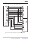
As an example, the following sections describe how to configure each of these registers for access to two
1Gb, 16-bit wide DDR2 SDRAM devices connected as shown on Figure 16, where each device has the
following configuration:
• Maximum data rate: 533MHz
• Number of banks: 8
• Page size: 1024 words
• CAS latency: 4
It is assumed that the frequency of the DDR2 memory controller clock (DDR2CLKOUT) is set to 250MHz.
3.2.1 Programming the SDRAM Configuration Register (SDCFG)
The SDRAM configuration register (SDCFG) contains register fields that configure the DDR2 memory
controller to match the data bus width, CAS latency, number of banks, and page size of the attached
DDR2 memory.
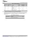
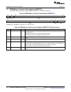
Table 11 shows the resulting SDCFG configuration. Note that the value of the TIMUNLOCK field is
dependent on whether or not it is desirable to unlock SDTIM1 and SDTIM2. The TIMUNLOCK bit should
only be set to 1 when the SDTIM1 and SDTIM2 needs to be updated.
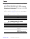
Table 11. SDCFG Configuration
Field Value Function Selection
TIMUNLOCK x Set to 1 to unlock the SDRAM timing and timing 2 registers. Cleared to 0 to lock the SDRAM
timing and timing 2 registers.
NM 0h To configure the DDR2 memory controller for a 32-bit data bus width.
CL 4h To select a CAS latency of 4.
IBANK 3h To select 8 internal DDR2 banks.
PAGESIZE 2h To select 1024-word page size.
3.2.2 Programming the SDRAM Refresh Control Register (SDRFC)
The SDRAM refresh control register (SDRFC) configures the DDR2 memory controller to meet the refresh
requirements of the attached DDR2 device. SDRFC also allows the DDR2 memory controller to enter and
exit self refresh. In this example, we assume that the DDR2 memory controller is not is in self-refresh
mode.
The REFRESH_RATE field in SDRFC is defined as the rate at which the attached DDR2 device is
refreshed in DDR2 cycles. The value of this field may be calculated using the following equation:
REFRESH_RATE = DDR2CLKOUT frequency × memory refresh period
35
SPRU970G–December 2005–Revised June 2011 C6455/C6454 DDR2 Memory Controller
Submit Documentation Feedback
Copyright © 2005–2011, Texas Instruments Incorporated