


www.ti.com
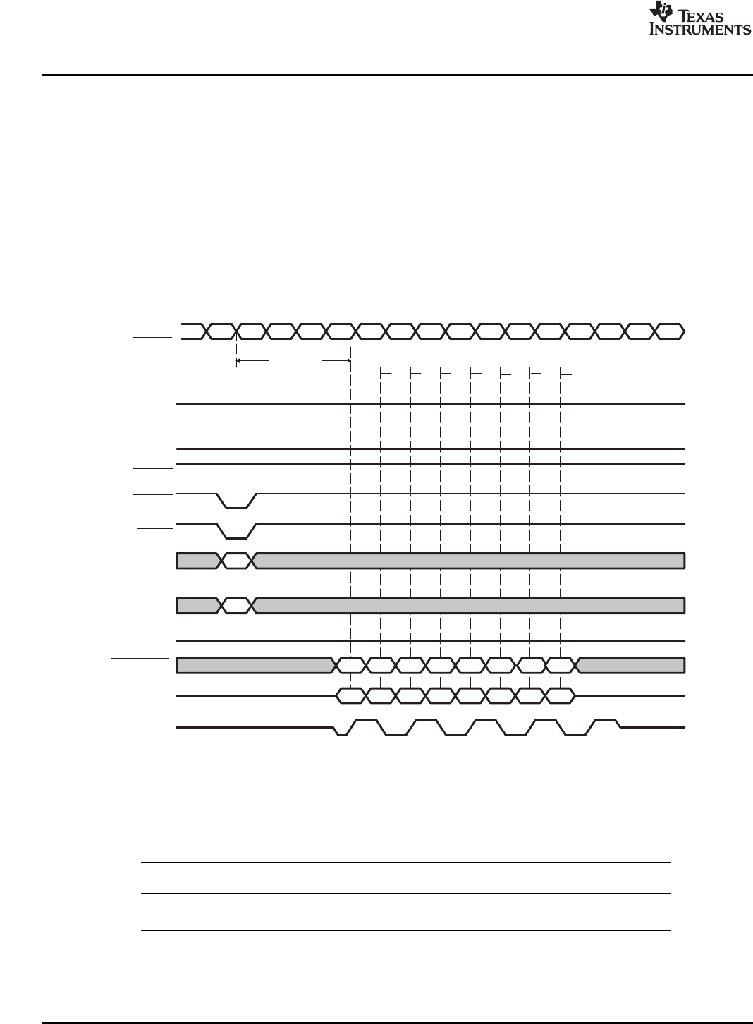
2.4.6Write(WRT)Command
DDR_D[31:0]
DDR_DQS[3:0]
COL
BANK
DQM7
Sample
D0 D1 D2 D3 D4 D5 D6 D7
DQM1 DQM2 DQM3 DQM4 DQM5 DQM6 DQM8
Write Latency
DDR_A[10]
DDR_CLK
DDR_CLK
DDR_CS
DDR_CKE
DDR_RAS
DDR_WE
DDR_DQM[3:0]
DDR_CAS
DDR_BA[2:0]
DDR_A[13:0]
2.5MemoryWidthandByteAlignment
PeripheralArchitecture
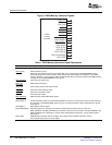
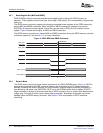
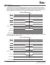
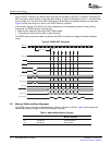
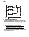
PriortoaWRTcommand,thedesiredbankandrowareactivatedbytheACTVcommand.Followingthe
WRTcommand,awritelatencyisincurred.WritelatencyisequaltoCASlatencyminus1.Allwriteshave
aburstlengthof8.TheuseoftheDDR_DQMoutputsallowsbyteandhalfwordwritestobeexecuted.
Figure9showsthetimingforawriteontheDDR2memorycontroller.
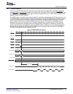
Ifthetransferrequestisforlessthan8words,dependingontheschedulingresultandthepending
commands,theDDR2memorycontrollercan:
•MaskouttheadditionaldatausingDDR_DQMoutputs
•Terminatethewriteburstandstartanewwriteburst
TheDDR2memorycontrollerdoesnotperformtheDEACcommanduntilpageinformationbecomes
invalid.
Figure9.DDR2WRTCommand
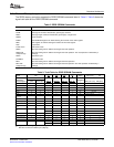
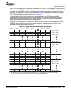
TheDDR2memorycontrollersupportsmemorywidthsof16bitsand32bits.Table4summarizesthe
addressablememoryrangesontheDDR2memorycontroller.
Table4.AddressableMemoryRanges
MemoryWidthMaximumAddressableBytesAddressTypeGeneratedbyDDR2
MemoryController
×16128MbytesHalfwordaddress
×32256MbytesWordaddress
DSPDDR2MemoryController 18SPRUEK5A–October2007
SubmitDocumentationFeedback