


www.ti.com
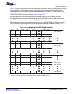
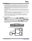
Col. 0 Col. 1 Col. 2 Col. 3 Col. 4 Col. M−1 Col. M
Row 0, bank 0
Row 0, bank 1
Row 0, bank 2
Row 0, bank P
Row 1, bank 1
Row 1, bank 0
Row 1, bank 2
Row 1, bank P
Row N, bank 2
Row N, bank 1
Row N, bank 0
Row N, bank P
PeripheralArchitecture
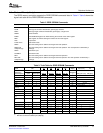
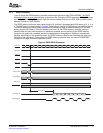
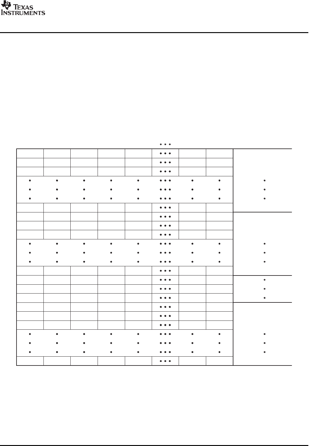
Figure11showshowtheDSPmemorymapispartitionedintocolumns,rows,andbanks.Notethatduring
alinearaccess,theDDR2memorycontrollerincrementsthecolumnaddressasthelogicaladdress
increments.WhentheDDR2memorycontrollerreachesapage/rowboundary,itmovesontothesame
page/rowinthenextbank.Thismovementcontinuesuntilthesamepagehasbeenaccessedinallbanks.
TotheDDR2SDRAM,thisprocesslooksasshownonFigure14.
Bytraversingacrossbankswhileremainingonthesamerow/page,theDDR2memorycontroller
maximizesthenumberofactivatedbanksforalinearaccess.Thisresultsinthemaximumnumberof
openpageswhenperformingalinearaccessbeingequaltothenumberofbanks.NotethattheDDR2
memorycontrollerneveropensmorethanonepageperbank.
EndingthecurrentaccessisnotaconditionthatforcestheactiveDDR2SDRAMrow/pagetobeclosed.
TheDDR2memorycontrollerleavestheactiverowopenuntilitbecomesnecessarytocloseit.This
decreasesthedeactivate-reactivateoverhead.
Figure13.LogicalAddress-to-DDR2SDRAMAddressMap
AMisnumberofcolumns(asdeterminedbyPAGESIZE)minus1,Pisnumberofbanks(asdeterminedbyIBANK)
minus1,andNisnumberofrows(asdeterminedbybothPAGESIZEandIBANK)minus1.
SPRUEK5A–October2007DSPDDR2MemoryController21
SubmitDocumentationFeedback