


Programming Model
MVME2500 Installation and Use (6806800L01H)
120
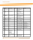
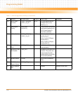
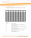
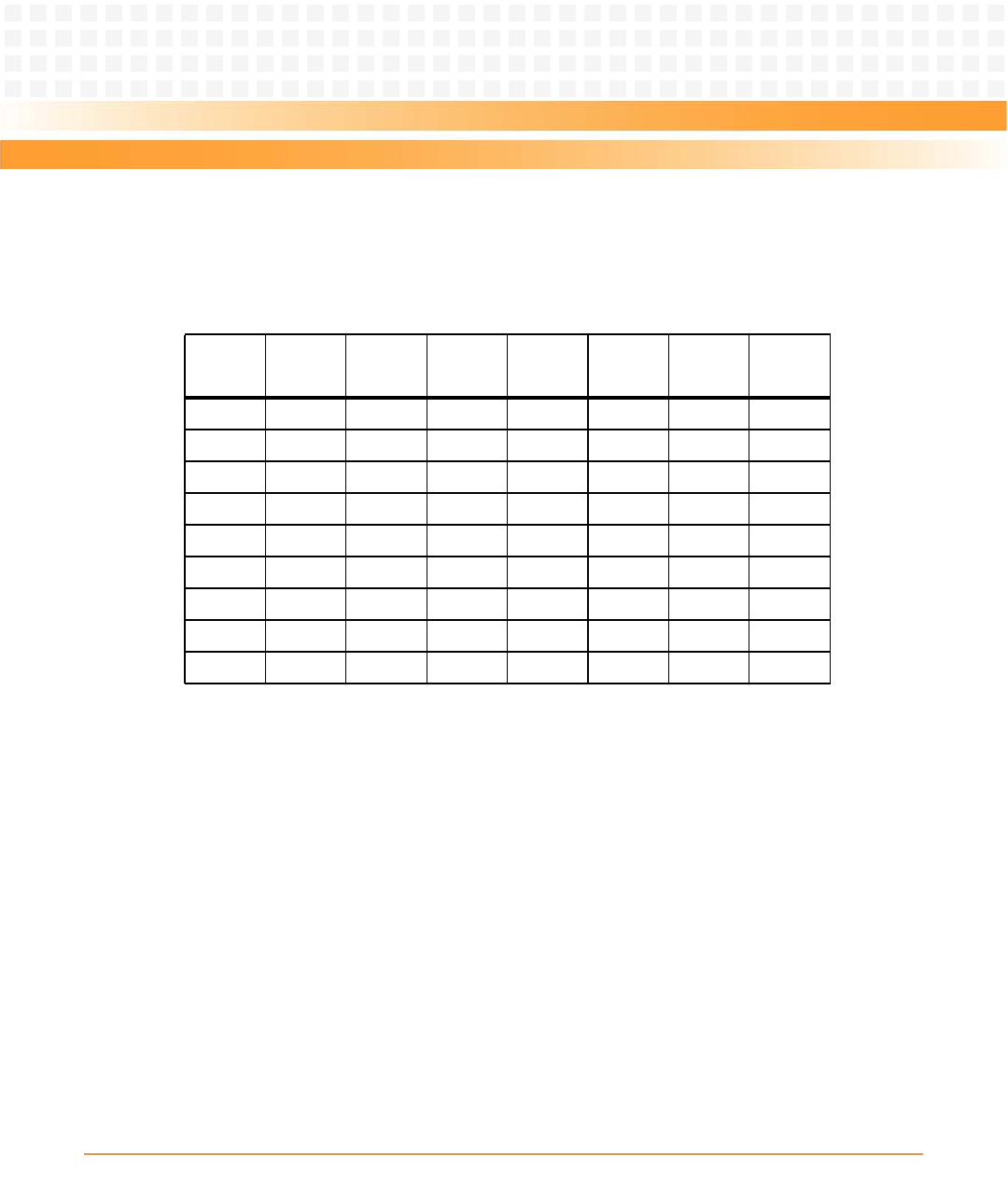
7.6.4 LBC Timing Parameters
The following table defines the timing parameters for the devices on the local bus.
Table 7-5 LBC Timing Parameters
0123456
MRAM UART 0 UART 1 UART 2 UART 3 FPGA Timers
BCTLD0000000
CSNT1111111
ACS10101010101010
XACS0000000
SCY 0011 0011 0011 0011 0011 0011 0011
SETA0000000
TRLX 0000000
EHTR 0000000
EAD0000000
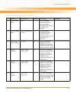
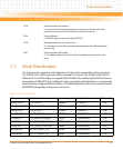
Field Description
BCTLD Buffer control disable.
0 - LBCTL is asserted upon access to the current memory bank.
CSNT Chip Select negation time.
1 - LCSn and LWE are negated one quarter of the bus clock cycle earlier
ACS Address to chip-select setup.
10 - LCSn is outputted one quarter bus clock cycle after the address lines.
XACS Extra Address to chip-select setup
0 - Address to chip-select setup is determined by ORx[ACS]
SCY Cycle length in bus clocks
0011 - Three bus clock cycle wait state