


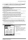

EVALUATION BOARD S5U1C62XXXE
S1C62 FAMILY EPSON VII-5
DEVELOPMENT TOOL REFERENCE MANUAL
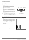
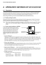
4.3 Under Top Cover
The layout and content within the top cover will vary depending on the model.
The below content is laid out here in a basic manner. Refer to the "S5U1C62xxxE Manual" for details.
• RESET switch
This switch resets the CPU and starts the target program from page 01H, step 00H.
• VADJ
This is the control for adjusting the LCD contrast.
(Refer to the "S5U1C62xxxE Manual".)
• VSVD
This is the control for varying the power supply voltage in simulation to check SVD operation.
(Refer to the "S5U1C62xxxE Manual".)
This control is not present in models that do not have the SVD function.
• DONE
This LED lights when the S5U1C62xxxE has completed configuration at power-on and is ready for
debugging. If this LED is not lit several seconds after power-on, switch the power off and then on again.
• F.HEX (ROM sockets)
This is the IC socket into which the ROM (F.HEX) is inserted. This ROM includes the function options
generated by the function option generator (FOG62XX).
• LED and CHK pin
LEDs that display the value ("1" or "0") of the special I/O registers and a terminals for confirmation by
oscilloscope or a like device have been provided.
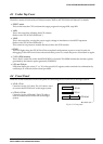
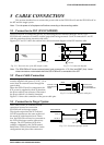
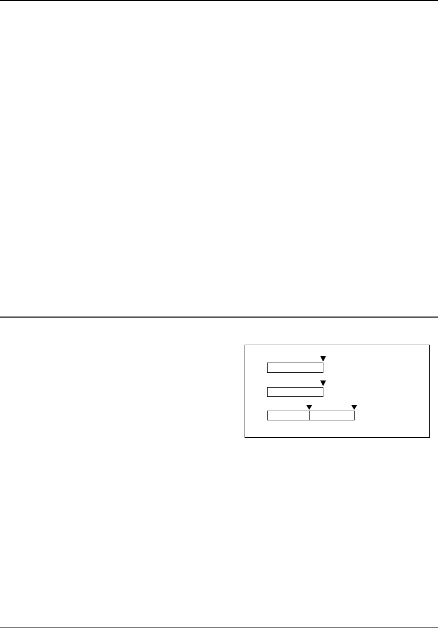
4.4 Front Panel
There are several connectors on the front panel for connecting the S5U1C62xxxE to the target system.
I/O #0
I/O #1
LCD #0, #1
▼ Position of pin 1
Fig. 4.4.1 Front panel
• I/O #0, I/O #1
Connector for the I/O cable. The I/O cable is used
to connect the S5U1C62xxxE to the target system.
• LCD #0, LCD #1
Connector for the LCD cable. The LCD cable is
used to connect the S5U1C62xxxE to the target
system.