Intel® Xeon® Processor E5-1600 v2/E5-2600 v2 Product Families 63
Datasheet Volume One of Two
Interfaces
2. The PECI host must determine the total number of machine check banks and the validity of the MCi_ADDR and MCi_MISC
register contents prior to issuing a read to the machine check bank similar to standard machine check architecture
enumeration and accesses.
3. The information presented in Table 2-11 is applicable to the processor only. No association between bank numbers and logical
functions should be assumed for any other processor devices (past, present or future) based on the information presented in
Table 2-11.
4. The processor machine check banks 4 through 19 reside in the processor uncore and hence will return the same value
independent of the processor ID used to access these banks.
5. The IA32_MCG_STATUS, IA32_MCG_CONTAIN and IA32_MCG_CAP are located in the uncore and will return the same value
independent of the processor ID used to access them.
6. The processor machine check banks 0 through 3 are core-specific. Since the processor ID is thread-specific and not core-
specific, machine check banks 0 through 3 will return the same value for a particular core independent of the thread
referenced by the processor ID.
7. PECI accesses to the machine check banks may not be possible in the event of a core hang. A warm reset of the processor
may be required to read any sticky machine check banks.
8. Valid processor ID values may be obtained by using the enumeration methods described in Section 2.5.2.7.2.
9. Reads to a machine check bank within a core or thread that is disabled will return all zeroes with a completion code of 0x90.
10. For SKUs where Intel QPI is disabled or absent, reads to the corresponding machine check banks will return all zeros with a
completion code of 0x40.
11. Greyed out services are reserved: MC6, MC8, MC13, MC14, MC15, MC16
2.5.2.8 RdPCIConfig()
The RdPCIConfig() command provides sideband read access to the PCI configuration
space maintained in downstream devices external to the processor. PECI originators
may conduct a device/function/register enumeration sweep of this space by issuing
reads in the same manner that the BIOS would. A response of all 1’s may indicate that
the device/function/register is unimplemented even with a ‘passing’ completion code.
Alternatively, reads to unimplemented registers may return a completion code of 0x90
indicating an invalid request. Responses will follow normal PCI protocol.
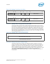
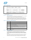
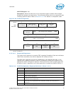
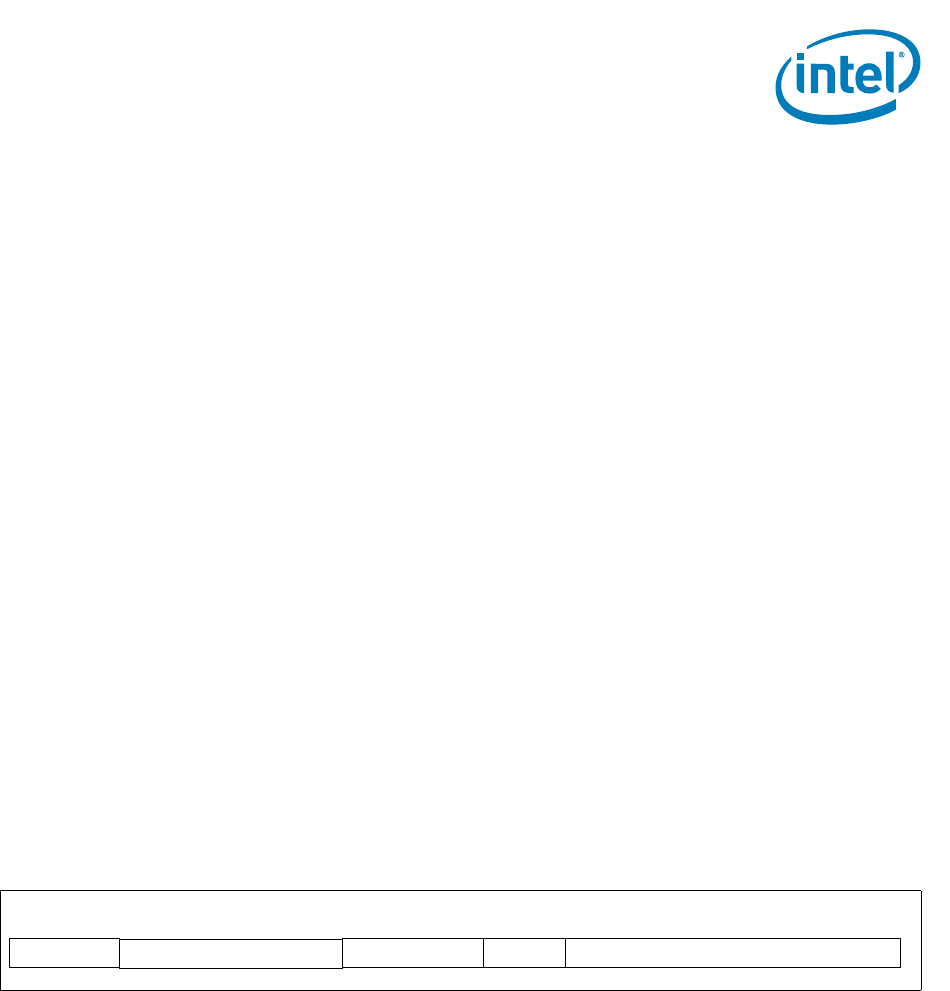
PCI configuration addresses are constructed as shown in Figure 2-44. Under normal in-
band procedures, the Bus number would be used to direct a read or write to the proper
device. Actual PCI bus numbers for all PCI devices including the PCH are programmable
by BIOS. The bus number for PCH devices may be obtained by reading the CPUBUSNO
CSR. Refer to the Intel® Xeon® Processor E5 v2 Product Family Processor Datasheet,
Volume Two: Registers document for details on this register.
PCI configuration reads may be issued in byte, word or dword granularities.
2.5.2.8.1 Command Format
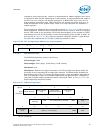
The RdPCIConfig() format is as follows:
Write Length: 0x06
Read Length: 0x05 (dword)
Command: 0x61
Description: Returns the data maintained in the PCI configuration space at the
requested PCI configuration address. The Read Length dictates the desired data return
size. This command supports only dword responses with a completion code on the
processor PECI clients. All command responses are prepended with a completion code
that includes additional pass/fail status information. Refer to Section 2.5.5.2 for details
regarding completion codes.
Figure 2-44. PCI Configuration Address
31
Reserved
2728 20 19 15 1114 12 0
FunctionDevice
Bus
Register


