Intel® Server Boards S5000PSL and S5000XSL TPS Design and Environmental Specifications
Revision 1.2
Intel order number: D41763-003
83
8.3.4 Voltage Regulation
The power supply output voltages must stay within the following voltage limits when operating at
steady state and dynamic loading conditions. These limits include the peak-peak ripple / noise.
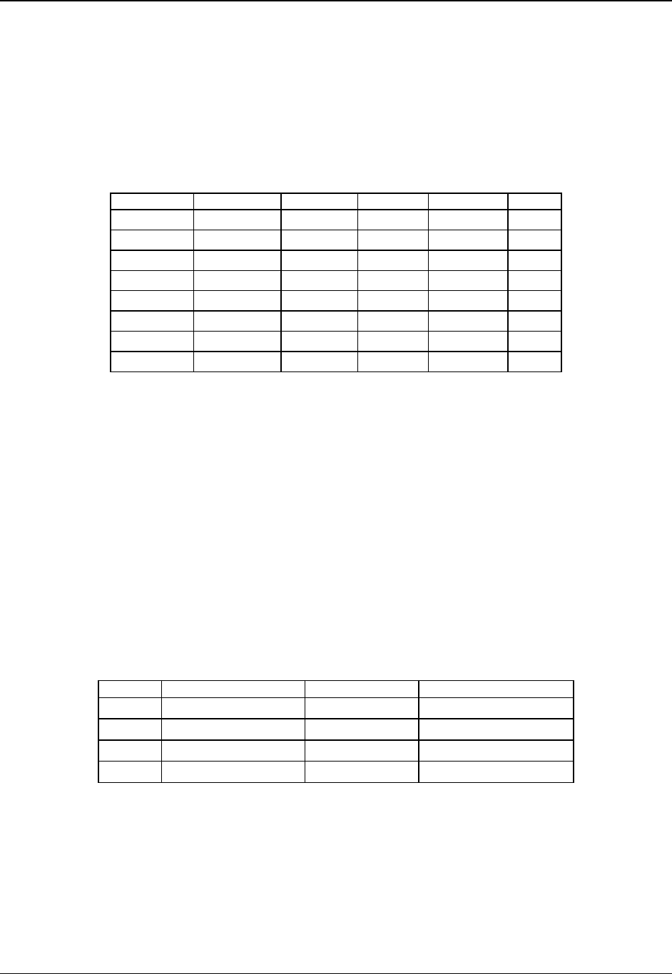
Table 40. Voltage Regulation Limits
Parameter Tolerance Minimum Nominal Maximum Units
+3.3V - 5% / +5% +3.14 +3.30 +3.46 V
rms
+5V - 5% / +5% +4.75 +5.00 +5.25 V
rms
+12V
1
- 5% / +5% +11.40 +12.00 +12.60 V
rms
+12V
2
- 5% / +5% +11.40 +12.00 +12.60 V
rms
+12V
3
- 5% / +5% +11.40 +12.00 +12.60 V
rms
+12V
4
- 5% / +5% +11.40 +12.00 +12.60 V
rms
- 12V - 5% / +9% - 11.40 -12.00 -13.08 V
rms
+5VSB - 5% / +5% +4.75 +5.00 +5.25 V
rms
1. Maximum continuous total output power should not exceed 670 W.
2. Maximum continuous load on the combined 12 V output shall not exceed 48 A.
3. Peak load on the combined 12 V output shall not exceed 52 A.
4. Peak total DC output power should not exceed 730 W.
8.3.5 Dynamic Loading
The output voltages shall remain within limits for the step loading and capacitive loading
specified in the table below. The load transient repetition rate shall be tested between 50 Hz
and 5 kHz at duty cycles ranging from 10%-90%. The load transient repetition rate is only a test
specification. The Δ step load may occur anywhere within the minimum load to the maximum
load conditions.
Table 41. Transient Load Requirements
Output
Δ Step Load Size
1
Load Slew Rate Test Capacitive Load
+3.3V 7.0A
0.25 A/μsec 4700 μF
+5V 7.0A
0.25 A/μsec 1000 μF
+12V 25A
0.25 A/μsec 4700 μF
+5VSB 0.5A
0.25 A/μsec 20 μF
1. Step loads on each 12V output may happen simultaneously.


