


Design and Environmental Specifications Intel® Server Boards S5000PSL and S5000XSL TPS
Revision 1.2
Intel order number: D41763-003
84
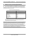
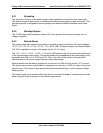
8.3.6 Capacitive Loading
The power supply shall be stable and meet all requirements with the following capacitive
loading ranges.
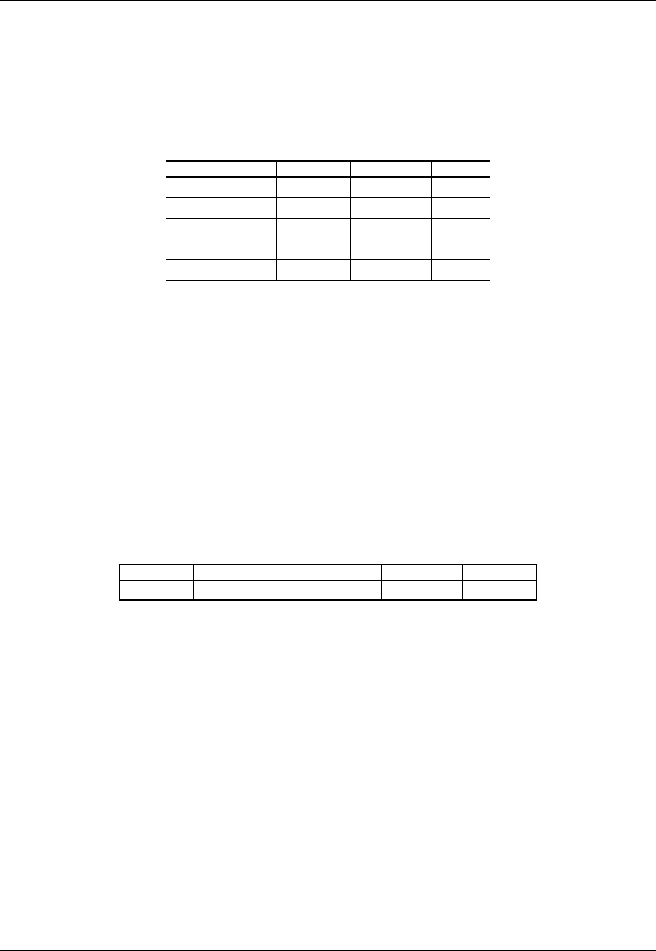
Table 42. Capacitive Loading Conditions
Output Minimum Maximum Units
+3.3 V 250 6800
μF
+5 V 400 4700
μF
+12 V
1, 2, 3, 4
500 each 11,000
μF
-12 V 1 350
μF
+5 VSB 20 350
μF
1. Maximum continuous total output power should not exceed 670 W.
2. Maximum continuous load on the combined 12 V output shall not exceed 48 A.
3. Peak load on the combined 12 V output shall not exceed 52 A.
4. Peak total DC output power should not exceed 730 W.
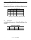
8.3.7 Ripple / Noise
The maximum allowed ripple/noise output of the power supply is defined in the following table.
This is measured over a bandwidth of 0Hz to 20MHz at the power supply output connectors. A
10 μF tantalum capacitor in parallel with a 0.1 μF ceramic capacitor are placed at the point of
measurement.
Table 43. Ripple and Noise
+3.3 V +5 V +12 V
1, 2, 3, 4
-12 V +5 VSB
50mVp-p 50mVp-p 120mVp-p 120mVp-p 50mVp-p
1. Maximum continuous total output power should not exceed 670 W.
2. Maximum continuous load on the combined 12 V output shall not exceed 48 A.
3. Peak load on the combined 12 V output shall not exceed 52 A.
4. Peak total DC output power should not exceed 730 W.
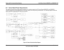
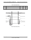
8.3.8 Timing Requirements
The following are the timing requirements for the power supply operation. The output voltages
must rise from 10% to within regulation limits (T
vout_rise
) within 5 to 70 ms. 5 VSB is allowed to
rise from 1.0 to 25 ms. All outputs must rise monotonically. Each output voltage shall reach
regulation within 50 ms (T
vout_on
) of each other during turn on of the power supply. Each output
voltage shall fall out of regulation within 400 msec (T
vout_off
) of each other during turn off.
The following tables and diagrams show the timing requirements for the power supply being
turned on and off via the AC input with PSON held low, and the PSON signal with the AC input
applied.