


86
80
80
50QMA
50QMA
N/B Maintenance
N/B Maintenance
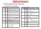
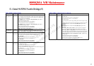
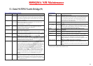
5.1 Intel 915PM North Bridge(9)
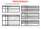
PLL Signals
Signal Name Type Description
HCLKP I
Diff Clk
Differential Host Clock In:
Differential clock input for the Host PLL. Used for phase cancellation
for FSB transactions. This clock is used by all of the GMCH logic
that is in the Host clock domain. Also used to generate core and
system memory internal clocks. This is a low voltage differential
signal and runs at ¼ the FSB data rate.
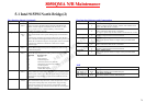
HCLKN I
Diff Clk
Differential Host Clock Input Complement:
GCLKP I
Diff Clk
Differential PCI Express based Graphics / DMI Clock In:
These pins receive a differential 100 MHz Serial Reference clock
from the external clock synthesizer. This clock is used to generate the
clocks necessary for the support of PCI Express.
GCLKN
I
Diff Clk
Differential PCI Express based Graphics / DMI Clock In
complement
DREF_CLKP I
Diff Clk
Display PLLA Differential Clock In –
Display PLL Differential Clock In, no SSC support –
DREF_CLKN I
Diff Clk
Display PLLA Differential Clock In Complement –
Display PLL Differential Clock In Complement - no SSC support
DREF_SSCLKP I
Diff Clk
Display PLLB Differential Clock In –
Optional Display PLL Differential Clock In for SSC support –
NOTE: Differential Clock input for optional SSC support for LVDS
display.
DREF_SSCLKN I
Diff Clk
Display PLLB Differential Clock In complement –
Optional Display PLL Differential Clock In Complement for SSC
support
NOT
E: Differential Clock input for optional SSC support for LVDS
display.
Note: PLL interfaces signal group are supported the Mobile Intel 915GM/PM/GMS and Intel
910GML Express chipsets, unless otherwise noted.
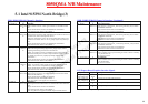
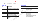
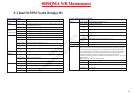
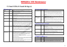
Reset and Miscellaneous Signals
Signal Name Type Description
RSTIN# I
HVCMOS
Reset In:
When asserted this signal will asynchronously reset the GMCH logic.
This signal is connected to the PLT_RST# output of the ICH6-M.
This input has a Schmitt trigger to avoid spurious resets. This input
buffer is 3.3-V tolerant.
PWROK I
HVCMOS
Power OK:
When asserted, PWROK is an indication to the GMCH that core
power has been stable for at least 10 µs.
This input buffer is 3.3-V tolerant.
H_BSEL [2:0]
(CFG[2:0])
I
HVCMOS
Host Bus Speed Select:
At the deassertion of RSTIN#, the value sampled on these pins
determines the expected frequency of the bus.
External pull-ups are required.
CFG[17:3] I
AGTL+
HW straps:
CFG [17:3] has internal pull up.
NOTE: Not all CFG Balls are supported for Intel 915GMS.
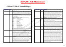
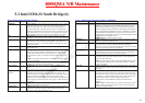
CFG[20:18]
I
HVCMOS
HW straps:
CFG [20:18] has internal pull down
NOTE: Not all CFG Balls are supported for Intel 915GMS.
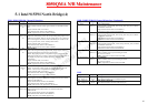
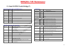
BM_BUSY# O
HVCMOS
GMCH Integrated Graphics Busy:
Indicates to the ICH that the integrated graphics engine within the
MCH is busy and transitions to low power states should not be
attempted until that is no longer the case.
THRMTRIP# O
COD
GMCH Thermal Trip:
Assertion of THERMTRIP# (Thermal Trip) indicates the GMCH
junction temperature has reached a level beyond which damage may
occur. Upon assertion of THERMTRIP#, the GMCH will shut off its
internal clocks (thus halting program execution) in an attempt to
reduce the GMCH core junction temperature. To protect GMCH, its
core voltage (Vcc) must be removed following the assertion of
THERMTRIP#. Once activated, THERMTRIP# remains latched
until RSTIN# is asserted. While the assertion of the RSTIN# signal
will deassert THERMTRIP#, if the GMCH’s junction temperature
remains at or above the trip level, THERMTRIP# will again be
asserted.
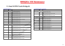
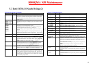
EXT_TS[1:0]# I
HVCMOS
External Thermal Sensor Input:
If the system temperature reaches a dangerously high value then this
signal can be used to trigger the start of system memory throttling.
NOTE: EXT_TS1# functionality is not supported in 915GMS. A pull
up is required on this pin
MiTac Secret
Confidential Document