


M30850T2-EPB User’s Manual 1. Outline
REJ10J1005-0200 Rev.2.00 April 1, 2007
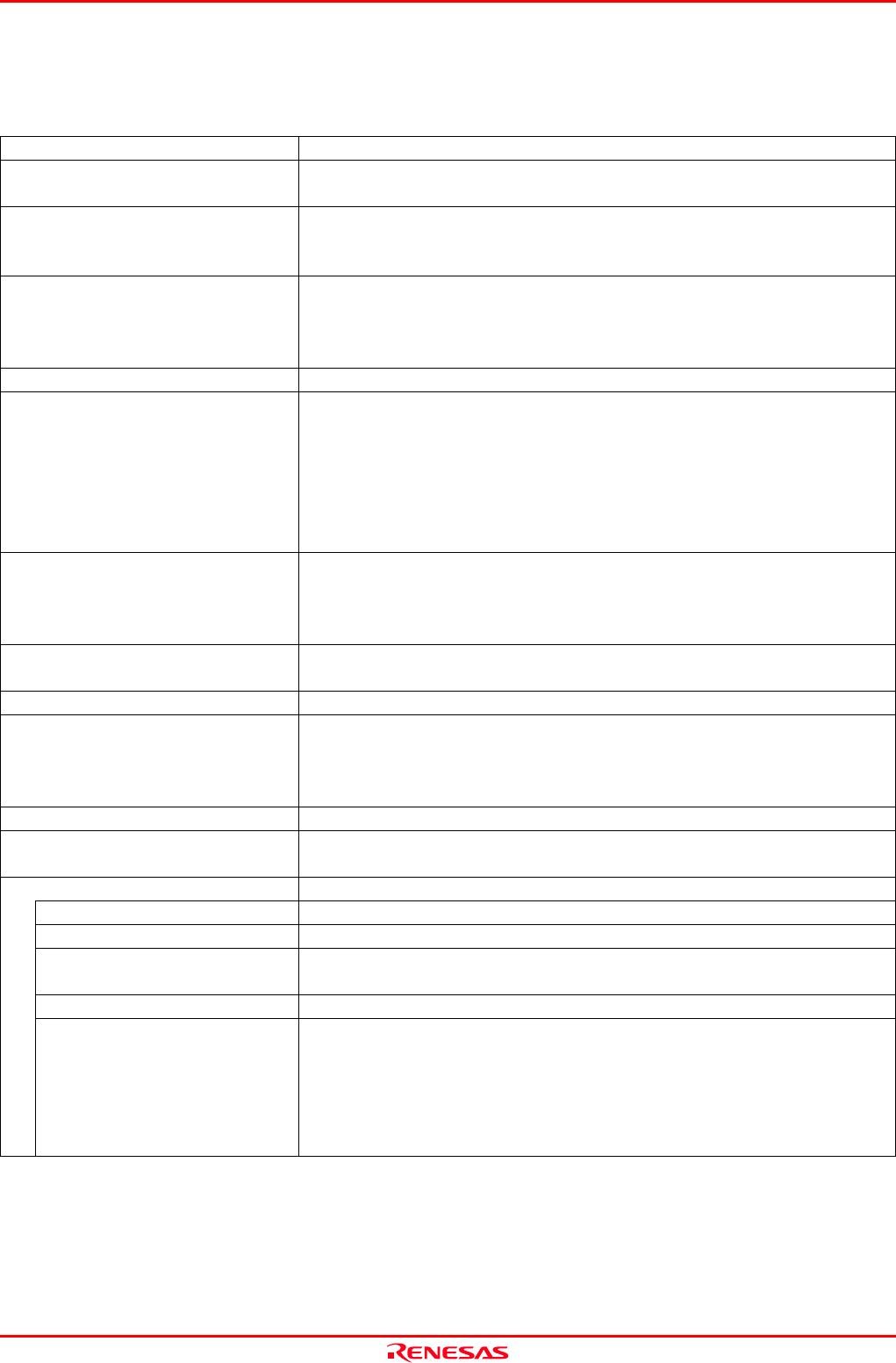
1.4 Specifications
Tables 1.5 and 1.6 list the specifications of the M30850T2-EPB.
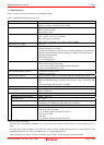
Table 1.5 M30850T2-EPB specifications (1/2)
Applicable MCUs M32C/80, 84, 85, 86 and 8A Groups
Evaluation MCU M30855FHGP
ROM size: 512 KB + 4 KB, RAM size: 24 KB
Usable mode Single-chip mode
Memory expansion mode
Microprocessor mode
Maximum operating frequency* VCC1 = VCC2 = 4.2 to 5.5 V: 32 MHz
VCC1 = VCC2 = 3.0 to 5.5 V: 24 MHz
Dual-power supply specification
(4.8V ≤ VCC1 ≤ 5.2V and 3.3V ≤ VCC2 ≤ VCC1): 32MHz
Applicable power supply 3.0--5.5 V
Basic debugging functions - Download
- Software break (max. 64 points)
- Program execution/stop (allows free-run execution supporting software breaks)
- Memory reference/setting (reference/setting C-variables, run-time execution)
- Register reference/setting
- Disassemble display
- C-level debugging, etc.
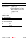
Real-time trace function - 256K-cycle bus information recordable
(Bus, external trigger, time stamp)
- 5 trace modes supported (Break/Before/About/After/Full)
- Can be recorded ON/OFF by events
Real-time RAM monitor function - 4,096 bytes (256 bytes x16)
- Data/last access result
Hardware break function 8 points (Execution address, bus detection, interrupt, external trigger signal)
Execution time measurement function Time between program start and stop
Maximum/minimum/average execution time and pass count of specified four
zones.
Count clock: Equal to MCU Clock or 16 MHz
C0 coverage 8,192 KB (256 KB x 32 blocks)
External trigger input/event output External trigger input (MCU-dependent-voltage CMOS level x8) or event output
(break x1, event x7)
Expansion emulation memory -
Maximum operating frequency 32 MHz 1Φ + 1Φ
Specifiable areas Max. 4 areas
Area size Contiguous 256 KB range or contiguous 1 MB range
(mixed setting of 256 KB range and 1 MB range is available)
Emulation memory size 4 MB for 4 areas
Specifiable bank - For area size 256 KB
X0h, X4h, X8h, XCh banks
e.g.) 20 bank, 64 bank, A8 bank, EC bank etc.
- For area size 1 MB
X0h hank
e.g.) 20 bank, 40 bank, 80 bank, A0 bank etc.
* Notes on Using This Product
- When the JP1 of the M30850T2-EPBM is set to VCC1>VCC2, the voltage of VCC2 on the user system should be 3.3 V or
more.
- If using a CPU clock of 30 MHz or more when the voltage of VCC1 is higher then that of VCC2, set the SFR area of the
intelligent I/O function to 2-wait (set the PM13 bit to "1") when reading this area.
These precautions only need to be observed when using an emulator, and do not apply for the actual MCU.
Page 17 of 98