M30850T2-EPB User’s Manual 3. Usage (How to Use the Emulator Debugger)
REJ10J1005-0200 Rev.2.00 April 1, 2007
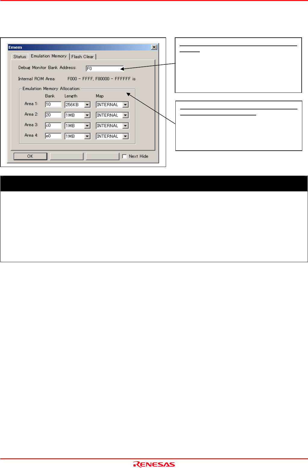
(2) Emulation Memory tab
1. Setting the Bank Address of the Debug Monitor
Setting the Bank Address of the Debug
Cancel Help
IMPORTANT
Notes on Setting a Debug Monitor Bank Address:
z It is not possible to view or set the content of the specified area. Even on the memory window or in the reverse
assemble area of the program/source windows, the content of this area is not displayed correctly though it can
be displayed.
z The below bank addresses cannot be set for the debug monitor.
(1) MCU internal resources (ROM, RAM and SFR areas)
(2) Multiplex areas
(3) Interrupt vector area
Monitor
The debug monitor uses contiguous 64 KB as a work area of
the emulator. Specify the bank address of the debug
monitor.
(e.g.: If F0 is specified, 64 KB area from D00000H address
is used by the debug monitor)
A
utomatically
A
llocating the Emulation
Memory of the Internal ROM
When selecting the single-chip mode or memory expansion
mode, an emulation memory is automatically allocated to an
internal ROM area. The automatically allocated addresses of
the internal ROM are shown here.
Page 55 of 98


