


M30850T2-EPB User’s Manual 4. Hardware Specifications
REJ10J1005-0200 Rev.2.00 April 1, 2007
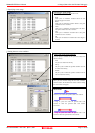
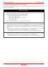
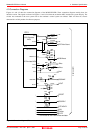
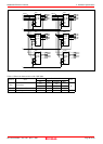
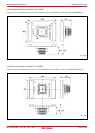
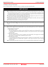
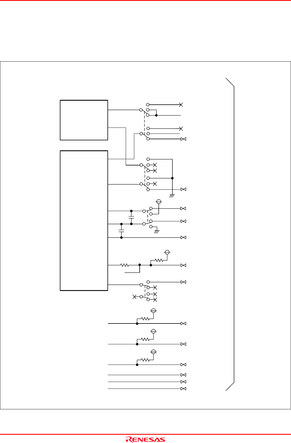
4.3 Connection Diagrams
Figures 4.1 and 4.2 show the connection diagrams of the M30850T2-EPB. These connection diagrams mainly show the
interface section. The signals not shown in Figures 4.1 and 4.2 connect the evaluation MCU and the user system directly. The
circuits not connected to the user system such as the emulator's control system are omitted. Table 4.2 shows IC electric
characteristics of this product for reference purposes.
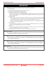
Figure 4.1 Connection diagram (1/2)
AVcc
Vref
AVss
P85/NMI*
CNVss
BYTE
P55/RDY*
P57/HOLD*
C1
C2
R17
R18
SW1
SW4
143
142
140
24
100
100k
*
R14
100k
*
RESET
*
R16
100k
*
R15
100k
*
XIN
*
XOUT
*
*
User system
IC1
I/O Emulate MCU
AVcc
Vref
AVss
P85/NMI*
P87/Xcin/Vcont
AVcc
Vcc
AVss
GND
XOUT
NC
*: Connected to the inside of the emulator.
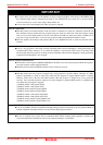
IC15
CPU Emulate
MCU
Vcc
P86/Xcout
SW2
18
17
*
P87/Xcin/Vcont
P86/Xcout
P86
NC
VSS
P87
XCIN
VCONT
Xcin
*
XCIN
VCONT
VSS
NC
NC
Xcout
SW3
17
18
Vcc
Vcc
Vcc
XOUT
20
NC
NC
NC
NC
NC
Page 79 of 98