


M30850T2-EPB User’s Manual 2. Setup
REJ10J1005-0200 Rev.2.00 April 1, 2007
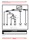
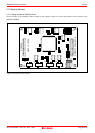
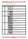
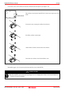
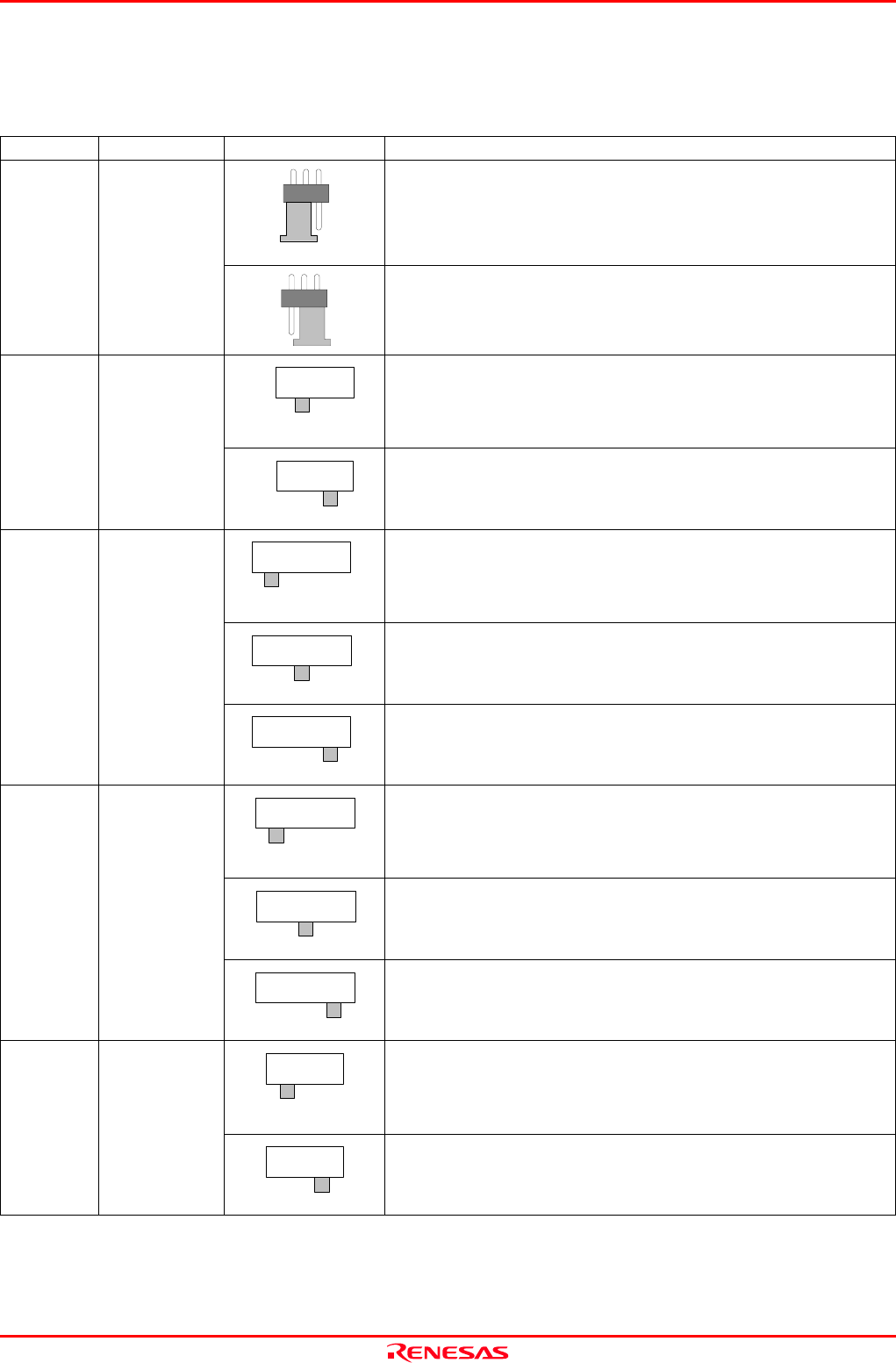
(1) Setting JP1, SW1 to SW4 on the M30850T2-EPBM
Table 2.2 shows the settings of JP1, SW1 to SW4 on the M30850T2-EPBM.
Table 2.2 Switch settings of the M30850T2-EPBM (JP1, SW1 to SW4)
Switch Switch name Setting Description
VCC1=2
VCC1>2
(Factory-setting)
3.0 V ≤ VCC1 = VCC2 ≤ 5.5 V
JP1* VDDIO
VCC1=2
VCC1>2
4.8 V ≤ VCC1 ≤ 5.2 V and 3.3 V ≤ VCC2 < VCC1
AVCC
AVSS
EXT
INT
(Factory-setting)
Connects pins AVCC and AVSS of the MCU to the user system.
SW1
AVCC
AVSS
AVCC
AVSS
EXT
INT
Connects pin AVCC of the MCU to the internal power supply of the
emulator, and connects pin AVSS to the GND in the emulator.
XCINP87 VCONT
(Factory-setting)
Connects pin P87 of the MCU to the user system.
XCINP87 VCONT
Connects pin P87 of the MCU to the sub-clock oscillator circuit
(32.768 kHz).
SW2 P87
XCINP87 VCONT
Do not set to VCONT.
Pin P87 is disconnected.
VSS
NCP86
(Factory-setting)
Connects pin P86 of the MCU to the user system.
VSS
NCP86
Does not connect pin P86 of the MCU.
SW3 P86
VSS
NCP86
Do not set to VSS.
Connects pin P86 to the VSS in the emulation probe.
XOUTNC
(Factory-setting)
Does not connect pin XOUT of the MCU.
SW4 XOUT
XOUTNC
Connects pin XOUT of the MCU to the user system.
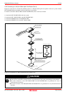
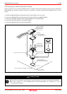
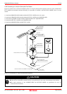
* Be careful about the direction when connecting.
Page 37 of 98