


M34571T2-CPE User’s Manual 4. Hardware Specifications
REJ10J0972-0100 Rev.1.00 February 10, 2006 Page 56 of 72
IMPORTANT
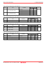
Note on Port Electrical Characteristics:
Because the following ports are configured with port emulation circuits, electrical characteristics differ from
those of the actual MCU.
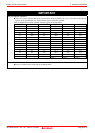
- P00--P03
- P10--P13
- P20--P21
- P30--P31
- D0--D3
- C
- K
- RESET#
For more details, refer to “4.3 Connection Diagram” (page 59).
The K, P20 and P21 pins, if pulled high in the user system, momentarily output a low after reset. This only
occurs after reset. To enable the evaluation MCU to be run in its exclusive mode, the pins on this product are
processed when reset. Although pin processing on this product is turned off after reset, the MCU is in the Hi-Z
state. This is why said difference occurs.
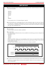
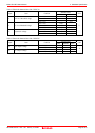
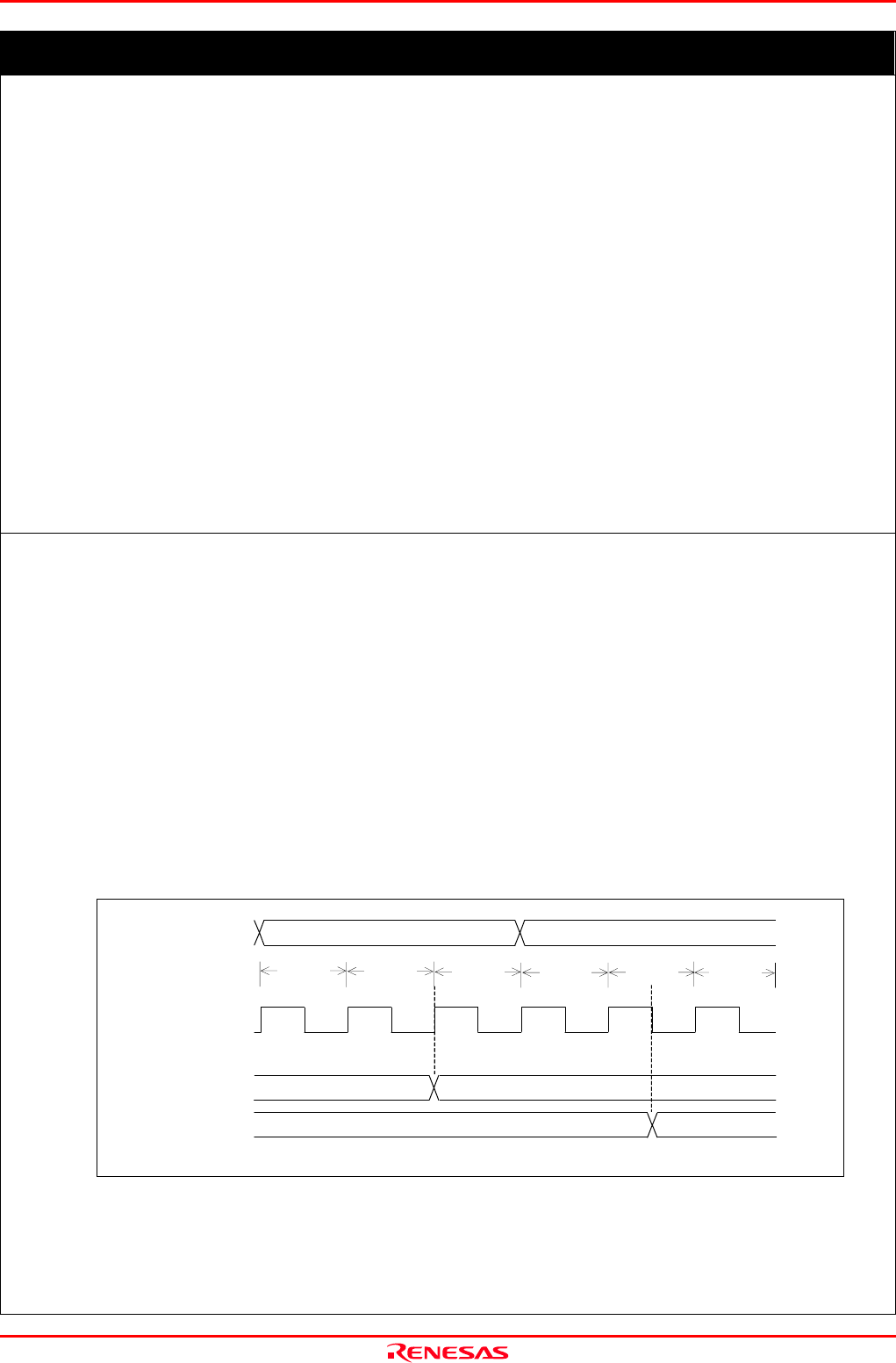
Notes on Port I/O Timings:
Port input timings
Port input timings are the same as with the actual MCUs.
Port output timings
Port output timings are different from those of the actual MCUs for the following ports that are configured with
port emulation circuits:
- P00--P03
- P10--P13
- P30--P31
- D0--D3
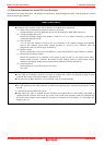
With the actual MCUs, changes occur at the beginning of the T3 state of an output instruction. With this
product, changes occur at the beginning of the T2 state of the next output instruction. Figure 4.1 shows the port
output timing for this product.
The output timings excluding the indicated above are the same as with the actual MCUs.
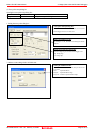
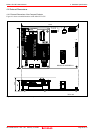
Figure 4.1 Port output timings
As a pitch converter board and other devices are used between the evaluation MCU and the user system. Some
characteristics are slightly different from those of the actual MCU. Therefore, be sure to evaluate your system
with an evaluation MCU.
Instruction
Cycle
XIN
Port output instruction
Next instruction
Port output of
actual MCU
Port output of
this product
T3
T1
T3
T2
T1 T2