


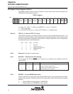

TMS380C26
NETWORK COMMPROCESSOR
SPWS010A–APRIL 1992–REVISED MARCH 1993
POST OFFICE BOX 1443 • HOUSTON, TEXAS
77251–1443
30
absolute maximum ratings over operating free-air temperature range (unless otherwise noted)
†
Supply voltage range, V
DD
(see Note 6) 7 V. . . . . . . . . . . . . . . . . . . . . . . . . . . . . . . . . . . . . . . . . . . . . . . . . . . . . . .
Input voltage range (see Note 6) – 0.3 V to 20 V. . . . . . . . . . . . . . . . . . . . . . . . . . . . . . . . . . . . . . . . . . . . . . . . . . .
Output voltage range – 2 V to 7 V. . . . . . . . . . . . . . . . . . . . . . . . . . . . . . . . . . . . . . . . . . . . . . . . . . . . . . . . . . . . . . . .
Power dissipation 1.0 W. . . . . . . . . . . . . . . . . . . . . . . . . . . . . . . . . . . . . . . . . . . . . . . . . . . . . . . . . . . . . . . . . . . . . . . .
Operating free-air temperature range 0°C to 70°C. . . . . . . . . . . . . . . . . . . . . . . . . . . . . . . . . . . . . . . . . . . . . . . . . .
Storage temperature range –65°C to 150°C. . . . . . . . . . . . . . . . . . . . . . . . . . . . . . . . . . . . . . . . . . . . . . . . . . . . . . .
†
Stresses beyond those listed under “absolute maximum ratings” may cause permanent damage to the device. These are stress ratings only and
functional operation of the device at these or any other conditions beyond those indicated under “recommended operating conditions” is not
implied. Exposure to absolute-maximum-rated conditions for extended periods may affect device reliability.
NOTE 6: Voltage values are with respect to V
SS
.
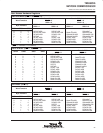
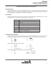
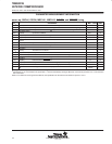
recommended operating conditions
MIN NOM MAX UNIT
V
DD
Supply voltage 4.75 5 5.25 V
V
SS
Supply voltage (see Note 7) 0 0 0 V
TTL-level signal 2.0 V
DD
+0.3
V
IH
High-level input voltage
OSCIN
†
2.6 V
DD
+0.3
V
RCLK, PXTALIN, RCVR 2.6 V
DD
+0.3
V
IL
Low level in
p
ut voltage TTL level signal (see Note 8)
OSCIN
‡
–0.3 0.6
V
V
IL
Lo
w-
le
v
el
inp
u
t
v
oltage
,
TTL
-
le
v
el
signal
(see
Note
8)
All other –0.3 0.8
V
I
OH
High level output current –400 µA
I
OL
Low level output current (see Note 9) 2 mA
T
A
Operating free-air temperature 0 70 °C
†
The minimum level specified is a result of the manufacturing test environment. This signal has been characterized to a minimum level of
2.4 V over the full temperature range.
‡
The maximum level specified is a result of the manufacturing test environment. This signal has been characterized to a maximum level of
0.8 V over the full temperature range.
NOTES: 7. All V
SS
pins should be routed to minimize inductance to system ground.
8. The algebraic convention, where the more negative (less positive) limit is designated as a minimum, is used in this data sheet for
logic voltage levels only.
9. Output current of 2 mA is sufficient to drive five low-power Schottky TTL loads or ten advanced low-power Schottky TTL loads (worst
case).
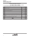
electrical characteristics over full ranges of recommended operating conditions (unless otherwise
noted)
PARAMETER
TEST CONDITIONS
(see Note 10)
MIN TYP MAX UNIT
V
OH
High-level output voltage, TTL-level signal (see Note 11) V
DD
= min, I
OH
= max 2.4 V
V
OL
Low-level output voltage, TTL-level signal V
DD
= min, I
OL
= max 0.6 V
I
O
High im
p
edance out
p
ut current
V
DD
= max, V
O
= 2.4 V 20
µA
I
O
High
-
impedance
o
u
tp
u
t
c
u
rrent
V
DD
= max, V
O
= 0.4 V – 20
µ
A
I
I
Input current, any input or input/output pin V
I
= V
SS
to V
DD
± 20 µA
I
DD
Supply current V
DD
= max 220 mA
C
i
Input capacitance, any input f = 1 MHz, other pins at 0 V 15 pF
C
o
Output capacitance, any output or input/output f = 1 MHz, other pins at 0 V 15 pF
NOTES: 10. For conditions shown as MIN or MAX, use the appropriate value specified under the recommended operating conditions.
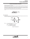
11. The following signals require an external pullup resistor: SRAS/SAS
, SRDY/SDTACK, SRD/SUDS, SWR/SLDS,
EXTINT0
–EXTINT3, and MBRQ.