


TMS380C26
NETWORK COMMPROCESSOR
SPWS010A–APRIL 1992–REVISED MARCH 1993
POST OFFICE BOX 1443 • HOUSTON, TEXAS
77251–1443
9
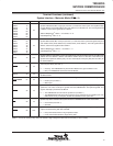
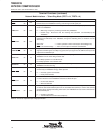
Terminal Functions (continued)
System Interface – Intel Mode (SI/M =H)
PIN NAME NO. I/O DESCRIPTION
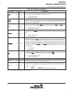
SADH0
SADH1
SADH2
SADH3
SADH4
SADH5
SADH6
SADH7
73
72
71
70
69
68
64
63
I/O
System Address/Data Bus—high byte (see Note 1).These lines make up the most significant byte
of each address word (32-bit address bus) and data word (16-bit data bus). The most significant bit
is SADH0, and the least significant bit is SADH7.
Address Multiplexing
†
: Bits 31 – 24 and bits 15 – 8.
Data Multiplexing
†
: Bits 15 – 8.
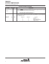
SADL0
SADL1
SADL2
SADL3
SADL4
SADL5
SADL6
SADL7
54
53
52
49
48
47
46
45
I/O
System Address/Data Bus—low byte (see Note 1). These lines make up the least significant byte of
each address word (32-bit address bus) and data word (16-bit data bus). The most significant bit is
SADL0, and the least significant bit is SADL7.
Address Multiplexing
†
: Bits 23 – 16 and bits 7 – 0.
Data Multiplexing
†
: Bits 7 – 0.
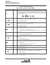
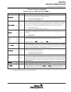
SALE 43 OUT
System Address Latch Enable. This is the enable pulse used to externally latch the 16 LSBs of the
address from the SADH0 – SADH7 and SADL0 – SADL7 buses at the start of the DMA cycle.
Systems that implement address parity can also externally latch the parity bits (SPH and SPL) for
the latched address.
SBBSY 31 IN
System Bus Busy. The TMS380C26 samples the value on this pin during arbitration. The sample has
one of (2) two values (see Note 1):
H = Not busy. The TMS380C26 may become Bus Master if the grant condition is met.
L = Busy. The TMS380C26 cannot become Bus Master.
SBCLK 44 IN
System Bus Clock. The TMS380C26 requires the external clock to synchronize its bus timings for
all DMA transfers.
SBHE/SRNW 57 I/O
System Byte High Enable. This pin is a three-state output that is driven during DMA and an input at
all other times.
H = System Byte High not enabled (see Note 1).
L = System Byte High enabled.
SBRLS
30 IN
System Bus Release. This pin indicates to the TMS380C26 that a higher-priority device requires the
system bus. The value on this pin is ignored when the TMS380C26 is
NOT
perfoming DMA. This
signal is internally synchronized to SBCLK.
H = The TMS380C26 can hold onto the system bus (see Note 1).
L = The TMS380C26 should release the system bus upon completion of current DMA cycle. If the
DMA transfer is not yet complete, the SIF will rearbitrate for the system bus.
SCS 29 IN
System Chip Select. Activates the system interface of the TMS380C26 for a DIO read or write.
H = Not selected (see Note 1).
L = Selected.
SDBEN 58 OUT
System Data Bus Enable. This output signals to the external data buffers to begin driving data. This
output is activated during both DIO and DMA.
H = Keep external data buffers in high-impedance state.
L = Cause external data buffers to begin driving data.
†
Typical bit ordering for Intel and Motorola processor buses.
NOTE 1: Pin has an internal pullup device to maintain a high voltage level when left unconnected (no etch or loads).