


TMS380C26
NETWORK COMMPROCESSOR
SPWS010A–APRIL 1992–REVISED MARCH 1993
POST OFFICE BOX 1443 • HOUSTON, TEXAS
77251–1443
33
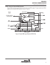
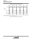
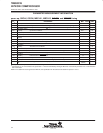
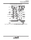
PARAMETER MEASUREMENT INFORMATION
timing parameters
The timing parameters for all the pins of TMS380C26 are shown in the following tables and are illustrated in the
accompanying figures. The purpose of these figures and tables is to quantify the timing relationships among
the various signals. The parameters are numbered for convenience.
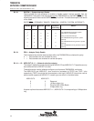
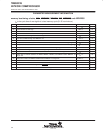
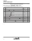
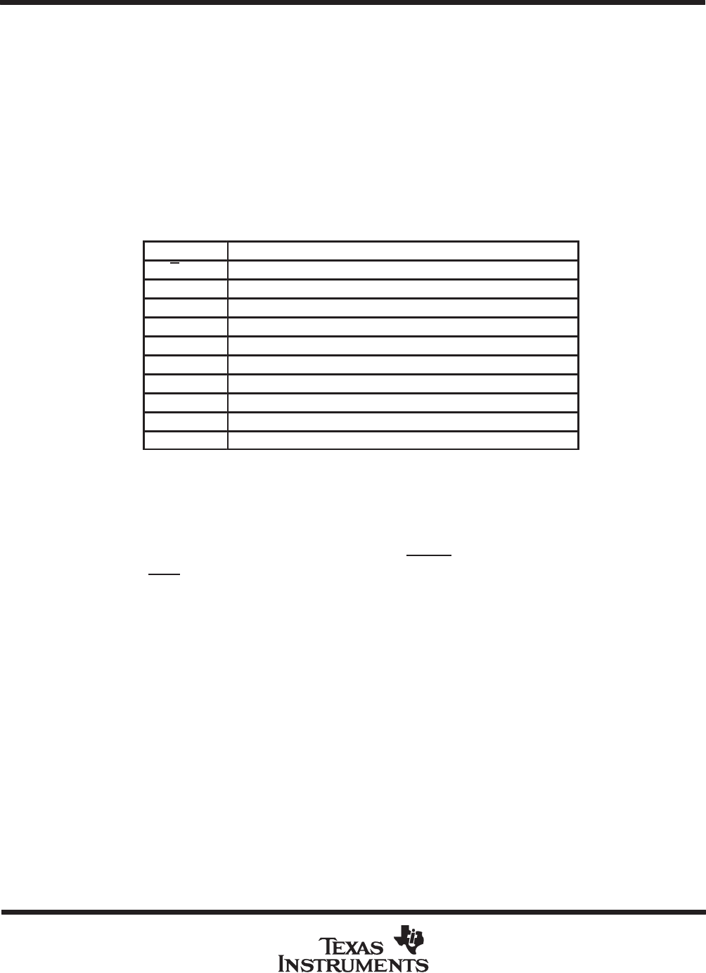
static signals
The following table lists signals that are not allowed to change dynamically and therefore have no timing
associated with them. They should be strapped high or low as required.
SIGNAL FUNCTION
SI/M Host processor select. (Intel/Motorola)
CLKDIV Reserved
BTSTRP Default bootstrap mode. (RAM/ROM)
PRTYEN Default parity select. (enabled/disabled)
TEST0 Test pin, indicates network type
TEST1 Test pin, indicates network type
TEST2 Test pin, indicates network type
TEST3 Test pin for TI manufacturing test.
†
TEST4 Test pin for TI manufacturing test.
†
TEST5 Test pin for TI manufacturing test.
†
†
For unit-in-place test.
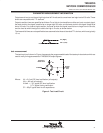
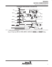
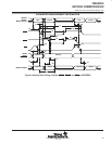
timing parameter symbology
Timing parameter symbols have been created in accordance with JEDEC standard 100. In order to shorten the
symbols, some of the pin names and other related terminology have been abbreviated as shown below:
DR DRVR RS SRESET
DRN DRVR VDD V
DDL
, V
DDB
OSC OSCIN
SCK SBCLK
Lower case subscripts are defined as follows:
c cycle time r rise time
d delay time sk skew
h hold time su setup time
w pulse duration (width) t transition time
The following additional letters and phrases are defined as follows:
H High Z High impedance
L Low Falling edge No longer high
V Valid Rising edge No longer low