


TMS380C26
NETWORK COMMPROCESSOR
SPWS010A–APRIL 1992–REVISED MARCH 1993
POST OFFICE BOX 1443 • HOUSTON, TEXAS
77251–1443
77
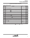
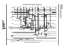
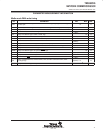
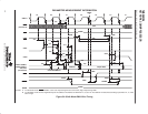
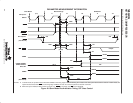
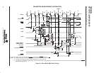
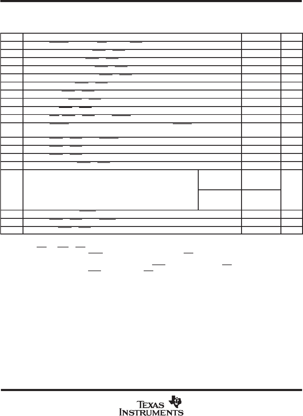
PARAMETER MEASUREMENT INFORMATION
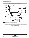
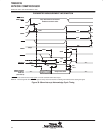
68xxx DIO write timing
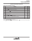
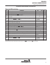
NO. PARAMETER MIN MAX UNIT
255 Delay from SDTACK low to either SCS, SUDS or SLDS high 15 ns
262 Setup of write data valid before SUDS or SLDS no longer low 25 ns
263 Hold of write data valid after SUDS or SLDS high 25 ns
267
§
Setup of register address before SUDS or SLDS no longer high (see Note 21) 15 ns
268 Hold of register address valid after SUDS or SLDS no longer low (see Note 22) 0 ns
272 Setup of SRNW before SUDS or SLDS no longer high (see Note 21) 15 ns
272a Setup of inactive SUDS or SLDS high to active data strobe no longer high 55 ns
273 Hold of SRNW after SUDS or SLDS high 0 ns
273a Hold of inactive SUDS or SLDS high after active data strobe high 55 ns
275 Delay from SCS, SUDS or SLDS high to SDTACK high (see Note 21) 35 ns
276
‡
Delay from SDTACK low in the first DIO access to the SIF register to SDTACK low in the
immediately following access to the SIF
4000 ns
279
†
Delay from SUDS or SLDS high to SDTACK high impedance 65 ns
280 Delay from SUDS or SLDS low to SDDIR low (see Note 21) 25 ns
281 Delay from SUDS or SLDS high to SDDIR high (see Note 21) 55 ns
281a Hold of SDDIR low after SUDS or SLDS no longer active (see Note 21) 0 ns
282b
Delay from SDBEN low to SDTACK low (see
TMS380 Second Generation Token-
If SIF register is
ready (no waiting
required)
0 35
ns
282b
y(
Ring User’s Guide,
SPWU005, subsection 3.4.1.1.1)
If SIF register is
not ready (waiting
required)
0 4000
ns
282W Delay from SDDIR low to SDBEN low 25 ns
283W Delay from SUDS or SLDS high to SDBEN no longer low 25 ns
286 Pulse duration, SUDS or SLDS high between DIO accesses (see Note 21) 55 ns
†
This specification is provided as an aid to board design.
‡
This specification has been characterized to meet stated value.
§
It is the later of SRD
and SWR or SCS low that indicates the start of the cycle.
NOTES: 21. The “inactive” chip select is SIACK
in DIO read and DIO write cycles, and SCS is the “inactive” chip select in interrupt acknowledge
cycles.
22. In 80x8x mode, SRAS may be used to strobe the values of SBHE
, SRSX, SRS0–SRS2, and SCS. When used to do so, SRAS must
meet parameter 266a, and SBHE
, SRS0–SRS2, and SCS must meet parameter 264. If SRAS is strapped high, then parameters
266a and 264 are irrelevant, and parameter 268 must be met.