VXI Technology, Inc.
36 VM4016 Programming
DACDATA
DACLOAD#
DACCLK
TRIGLEV1
U8
DAC
CONTROL
+
-
4.7K
470K
1K
COMPCH1
4. 7K
VCC
BUFCH1
(FRONT PANEL
CONNECTOR)
U13A
U3
+
-
10pf
2K
6K
100K
10K
100K
100K
+CH1
-CH1
U17A
K9
100K
10K
K9
DATA 0-15
ADDRESS
0-5, 29
4. 7K
1K
10K
VCC
LATIRQOUT
Q34
RELAYCLK
RELAYDATA
RELAYENA*
U15
RELAY
DRIVER
TO RELAY K9
DOE*
CONTROL
DATA
CONTROL
IRQ*
VMIP
BUS
TO FRONT PANEL
CONNECTOR
DATA
BUFFER
CONTROL
BUFFER
U4
U1
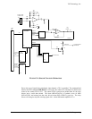
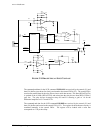
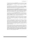
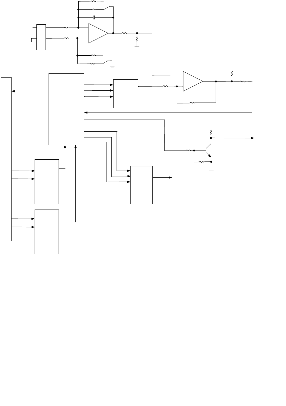
FIGURE 3-1: SINGLE CHANNEL OPERATION
Due to the type of signal being monitored, input channel +CH1 is grounded. The command and
data for the SCPI command INP:RANG is received by the control (U1) and data (U4) buffers and
routed to the control FPGA (U3). The control FPGA converts the parallel data for the relay
drivers into a serial data stream. This data (RELAYDATA) is synched to the 10 MHz
(RELAYCLK) and written into the relay drivers when (RELAYENA*) goes low. The relay
drivers will energize relay K9 selecting a gain of 0.1 for the differential amplifier U17A.


