www.vxitech.com
VM4016 Programming 39
DACDATA
DACLOAD#
DACCLK
TRIGLEV1
U8
DAC
CONTROL
+
-
4. 7K
470K
1K
COMPCH1
VCC
+
-
10pf
2K
6K
100K
10K
100K
100K
+CH1
-CH1
U17A
K9
100K
10K
K9
4. 7K
BUFCH1
U13A
U3
DATA 0-15
4.7K
1K
10K
VCC
IRQOUT
COMPCH2
TRIGLEV2
TRIGLEV2
VCC
+
-
10pf
2K
6K
100K
10K
100K
100K
+CH2
-CH2
U17B
K1
100K
10K
K1
+
-
4.7K
470K
1K
4. 7K
BUFCH2
U13B
IRQ*
CONTROL
TO
VMIP
BUS
Q33
INPUT
SIGNAL
FROM
FRONT
PANEL
CONNECTOR
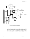
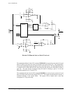
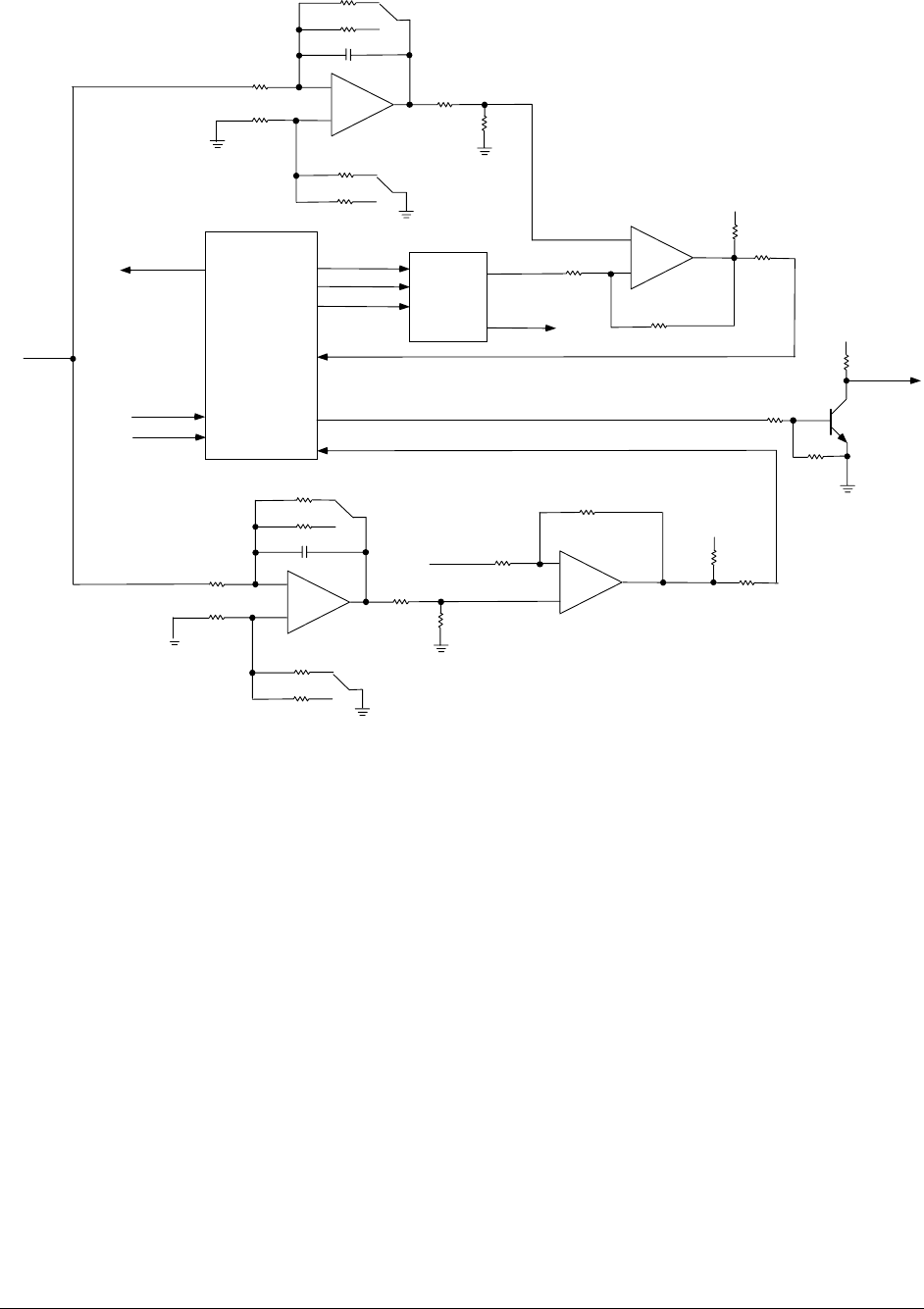
FIGURE 3-2: BRACKETING AN INPUT VOLTAGE
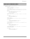
The command and data for the SCPI command INP:RANG are received by the control (U1) and
data (U4) buffers (not shown for clarity) and routed to the control FPGA (U3). The control FPGA
converts the parallel data for the relay drivers into a serial data stream. This data (RELAYDATA)
is synched to the 10 MHz (RELAYCLK) and written into the relay drivers when (RELAYENA*)
goes low. The relay drivers de-energize relays K9 and K1 selecting a gain of 1.0 for the
differential amplifiers at U17A and U17B.
The command and data for the SCPI command INP:DEB are received by the control (U1) and
data (U4) buffers and routed to the control FPGA (U3). The register for the debounce circuitry is
contained internally in the control FPGA. The register will be loaded with a value that
corresponds to a 750 µs time delay.


