VXI Technology, Inc.
88 VM4016 Theory of Operation
INPUT RANGE CONTROL
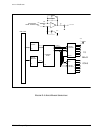
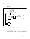
The Input Range or gain control for each of the sixteen channels is accomplished by U3, the
control FPGA, the data and command buffers U4 and U1, the relay drivers, U15 and U16 and
relays K1 through K16 (see Figure 5-1). The command to select the ±100 volt range is latched
into the data buffer at U4 and the control bits are latched into the command buffer at U1. The data
out enable line is driven low transferring the data and control bits to the control FPGA, U3. The
control FPGA decodes the control bits and drives the RELAYENA* signal low. This signal
enables the relay drivers, U15 and U16 to receive the incoming data and control signals.
U3 then converts the parallel data from the VMIP Bus to a 16-bit serial data word. This serial
data word (RELAYDATA) is synched to the 10 MHz gated relay clock (RELAYCLK) and sent to
the relay drivers. The relay drivers are cascaded so that the serial output from U15 feeds the serial
input of U16. The parallel outputs from the relay drivers will drive either low or high thereby
energizing or de-energizing the appropriate relays K1 through K16, in this case K9. The relay is
divided into three (3) sections for ease of analysis. The reference designator K9:A is given to the
relays coil, K9:B and K9:C are given to the relay's contacts. When energized the K9 relay selects
a 10 kΩ resistor on both of the inputs to the differential amplifier. This provides for a gain of 0.1
thus allowing for input voltage range of ± 100 V. When the K9 relay is de-energized it will
default to a 100 kΩ resistor that provides a gain of 1 thereby allowing ±10 V input voltage range.


