www.vxitech.com
VM4016 Programming 37
The command and data for the SCPI command INP:DEB is received by the control (U1) and data
(U4) buffers and routed to the control FPGA (U3). The register for the debounce circuitry is
contained internally in the control FPGA. The debounce register will be loaded with a value that
corresponds to a 250 ms time delay.
The commands and data for the SCPI commands INP:MASK are received by the control (U1)
and data (U4) buffers and routed to the control FPGA (U3). The mask register circuitry is
contained internally in the control FPGA. This register will be loaded so that Channels 2 through
16 are disabled or masked out.
The command for the SCPI command INP:POL is received by the control (U1) and data (U4)
buffers and routed to the control FPGA (U3). The mask register and debounce circuitry uses this
command to determine whether the input signal is an active high or an active low. The input
polarity has been programmed to NORM to cause U3 to treat the input signal as an active high.
The commands and data for the SCPI command INP:OFFS are received by the control (U1) and
data (U4) buffers and routed to the control FPGA (U3). The control FPGA will convert the
parallel data for the DAC (U8) into a serial data stream. This data (DACDATA) is synched to the
10 MHz gated clock (DACCLK) and loaded into the DAC when the (DACLOAD) signal goes
high.
The command for the SCPI command OUTP:POL:EXT:LATC is received by the control (U1)
and data (U4) buffers and routed to the control FPGA (U3). The latch register uses this command
to determine whether the output signal should be an active high or an active low. This was
programmed for INV to cause U3 to output an active low EXTLATIRQ signal to the front panel
connector when an interrupt occurs.
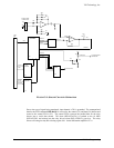
Now that the VM4016 is configured, it can be determined how this works. The output of the
differential amplifier U17A (BUFCH1) is voltage divided by 4. Since the gain of U17A is 0.1,
this makes BUFCH1 0.875 V when -CH1 reaches +35.0 V. BUFCH1 is compared with the
output of U8 (TRIGLEV1) by comparator U13A. When BUFCH1 is greater than TRIGLEV1 the
output of U13A (COMPCH1) goes low. COMPCH1 is routed to the debounce circuitry inside
U3.
The debounce circuitry will count down for 250 ms before clocking through COMPCH1. This
circuitry is used to mask out transients from generating false interrupts. When the 250 ms time
limit has expired, U3 clocks COMPCH1 into the mask register. The mask register will AND
COMPCH1 with the mask value (0001). The mask register passes COMPCH1 to a 16 input
OR’ing function that determines which Channel was first to cross its threshold. The output of this
OR’ing then latches into the “First Latch Register”. This signal, arbitrarily called
FIRSTLATCHED, clocks an internal latch that drives the base of Q34. Q34 conducts and drives
a low out on the front panel connector signal EXTLATIRQ. When an interrupt condition is
detected by U3 a VXI IRQ* is generated to the VMIP bus.


