


www.vxitech.com
VM4016 Theory of Operation 91
The input voltage or signal is applied to the non-inverting input of the differential amplifier,
U17A. The output voltage of U17A is divided by four (4) for compensation of the DAC’s full
range output of ±3 V.
Now that the flow of the circuitry has been established, it can be observed how the circuitry works
during normal operation. For this example the signal -CH1 will be tied to ground. A +5 VDC
digital supply line will be monitored for voltage surges in excess 0.25 V.
The DAC is loaded with the binary serial data word, 01101000. This provides a trigger level that
is 1.313 V. The +5V input signal +CH1, is applied to U17A’s non-inverting input. The output,
BUFCH1, of this amplifier is divided by 4, thus BUFCH1 is equal to +1.25V. This is compared
with the reference voltage, TRIGLEV1, of 1.313V. Since TRIGLEV1 is higher than BUFCH1
the comparator’s output, COMPCH1, remains at +5V. When the voltage on +CH1 exceeds
+5.25V BUFCH1 will then be higher than TRIGLEV1. This will drive the comparator to
saturation and COMPCH1 will equal 0 V.
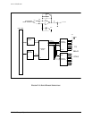
INTERRUPT GENERATION
All interrupt generation circuitry is contained within U3 the control FPGA. For the first part of
the interrupt generation section, Channel 1 (COMPCH1) polarity is normal. The input channel
signal inversion will be examined during the second part of this section. It will be assumed that
Channel 1 is the only activated channel and all others are masked out.
The command to specify the debounce time and input polarity is received in the data and
command buffers and subsequently transferred to the control FPGA at U3. The input signal
COMPCH1 has been compared with the reference voltage TRIGLEV1, as previously discussed,
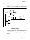
and is routed to the debounce circuitry inside U3 (see Figure 5-3). The debounce circuitry will
not allow COMPCH1 to pass through, unless it is low, for longer than the specified amount of
time. This circuitry is very useful in blocking out transients from generating false interrupt
requests. When the specified time limit has elapsed, and COMPCH1 is still active, it will then be
compared with the programmed value in the mask register. Since COMPCH1 is not masked out it
is then OR’ed with the remaining unmasked channels. The first channel (COMPCH1) to pass
through the debounce circuitry and mask register will latch into an internal register called “First
Latch Register”. This register is available to the user for determination of the interrupting
channel. COMPCH1 is used to clock an internal latch that in turn drives the “LATIRQOUT”
signal on the front panel connector. COMPCH1 is also used in the pulse generation circuitry that
generates the Interrupt Request (IRQOUT) pulse that is 500 ns wide.
When signal inversion is selected the interrupt will be generated when COMPCH1 is less than the
reference voltage TRIGLEV1. The debounce circuitry and the mask register use this signal INV
to determine polarity (see Figure 5-3). INV determines whether COMPCH1 is treated as an active
low for normal and active high for an inverted signal.