26 www.xilinx.com ML605 Hardware User Guide
UG534 (v1.2.1) January 21, 2010
Chapter 1: ML605 Evaluation Board
6. USB JTAG
JTAG configuration is provided through onboard USB-to-JTAG configuration logic where
a computer host accesses the ML605 JTAG chain through a Type-A (computer host side) to
Type-Mini-B (ML605 side) USB cable.
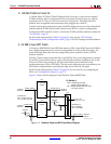
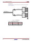
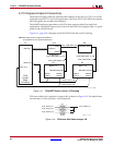
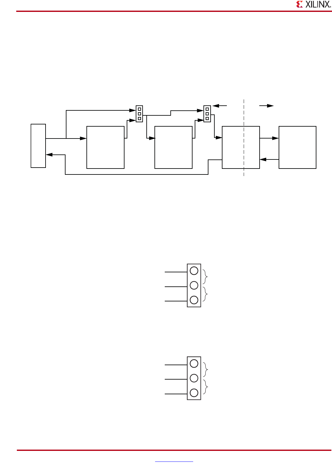
The JTAG chain of the board is illustrated in Figure 1-4. JTAG configuration is allowable at
any time under any mode pin setting. JTAG initiated configuration takes priority over the
mode pin settings.
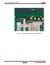
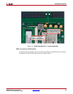
FMC bypass jumpers J17 and J18 must be connected between pins 1-2 (bypass) to enable
JTAG access to the FPGA on the basic ML605 board (without FMC expansion modules
installed), as shown in Figure 1-5 and Figure 1-6. When either or both VITA 57.1 FMC
expansion connectors are populated with an expansion module that has a JTAG chain, the
respective jumper(s) must be set to connect pins 2-3 in order to include the FMC expansion
module's JTAG chain in the main ML605 JTAG chain.
X-Ref Target - Figure 1-4
Figure 1-4: JTAG Chain Diagram
J22
USB Mini-B
FMC HPC FMC LPC
TDI TDO
J64
TDI
TDI
TDO
TDO
J63
J17 J18
3.3V 2.5V
System ACE CF FPGA
TSTTDI CFGTDO
TSTTDO CFGTDI
U19
U1
UG534_04_081309
X-Ref Target - Figure 1-5
Figure 1-5: VITA 57.1 FMC HPC (J64) JTAG Bypass Jumper J17
X-Ref Target - Figure 1-6
Figure 1-6: VITA 57.1 FMC LPC (J63) JTAG Bypass Jumper J18
J17
1
FMC_TDI_BUF
Bypass FMC HPC J64 = Jumper 1-2
Include FMC HPC J64 = Jumper 2-3
H - 1x3
UG534_05_081309
2
FMC_LPC_TDI
3
FMC_HPC_TDO
J18
1
FMC_LPC_TDI
Bypass FMC LPC J63 = Jumper 1-2
Include FMC LPC J63 = Jumper 2-3
H - 1x3
UG534_06_081309
2
SYSACE_TDI
3
FMC_LPC_TDO


