ML605 Hardware User Guide www.xilinx.com 79
UG534 (v1.2.1) January 21, 2010
Appendix C
ML605 Master UCF
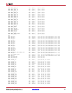
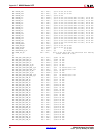
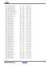
The UCF template is provided for designs that target the ML605. Net names provided in
the constraints below correlate with net names on the ML605 Rev. D schematic. On
identifying the appropriate pins, the net names below should be replaced with net names
in the user RTL. See the Constraints Guide
for more information.
Users can refer to the UCF files generated by tools such as MIG (Memory Interface
Generator for memory interfaces) and BSB (Base System Builder) for more detailed
information concerning the I/O standards required for each particular interface. The FMC
connectors J63 and J64 are connected to 2.5V V
cco
banks. Because each user’s FMC card
implements customer-specific circuitry, the FMC bank I/O standards must be uniquely
defined by each customer.
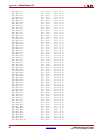
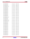
NET "CLK_33MHZ_SYSACE" LOC = "AE16"; ## 93 on U19
NET "CPU_RESET" LOC = "H10"; ## 2 on SW10 pushbutton (active-High)
##
NET "DDR3_A0" LOC = "L14"; ## 98 on J1
NET "DDR3_A1" LOC = "A16"; ## 97 on J1
NET "DDR3_A2" LOC = "B16"; ## 96 on J1
NET "DDR3_A3" LOC = "E16"; ## 95 on J1
NET "DDR3_A4" LOC = "D16"; ## 92 on J1
NET "DDR3_A5" LOC = "J17"; ## 91 on J1
NET "DDR3_A6" LOC = "A15"; ## 90 on J1
NET "DDR3_A7" LOC = "B15"; ## 86 on J1
NET "DDR3_A8" LOC = "G15"; ## 89 on J1
NET "DDR3_A9" LOC = "F15"; ## 85 on J1
NET "DDR3_A10" LOC = "M16"; ## 107 on J1
NET "DDR3_A11" LOC = "M15"; ## 84 on J1
NET "DDR3_A12" LOC = "H15"; ## 83 on J1
NET "DDR3_A13" LOC = "J15"; ## 119 on J1
NET "DDR3_A14" LOC = "D15"; ## 80 on J1
NET "DDR3_A15" LOC = "C15"; ## 78 on J1
NET "DDR3_BA0" LOC = "K19"; ## 109 on J1
NET "DDR3_BA1" LOC = "J19"; ## 108 on J1
NET "DDR3_BA2" LOC = "L15"; ## 79 on J1
NET "DDR3_CAS_B" LOC = "C17"; ## 115 on J1
NET "DDR3_CKE0" LOC = "M18"; ## 73 on J1
NET "DDR3_CKE1" LOC = "M17"; ## 74 on J1
NET "DDR3_CLK0_N" LOC = "H18"; ## 103 on J1
NET "DDR3_CLK0_P" LOC = "G18"; ## 101 on J1
NET "DDR3_CLK1_N" LOC = "L16"; ## 104 on J1
NET "DDR3_CLK1_P" LOC = "K16"; ## 102 on J1
NET "DDR3_D0" LOC = "J11"; ## 5 on J1
NET "DDR3_D1" LOC = "E13"; ## 7 on J1
NET "DDR3_D2" LOC = "F13"; ## 15 on J1
NET "DDR3_D3" LOC = "K11"; ## 17 on J1
NET "DDR3_D4" LOC = "L11"; ## 4 on J1
NET "DDR3_D5" LOC = "K13"; ## 6 on J1
NET "DDR3_D6" LOC = "K12"; ## 16 on J1
NET "DDR3_D7" LOC = "D11"; ## 18 on J1


