ML605 Hardware User Guide www.xilinx.com 37
UG534 (v1.2.1) January 21, 2010
Detailed Description
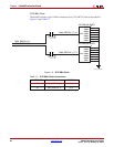
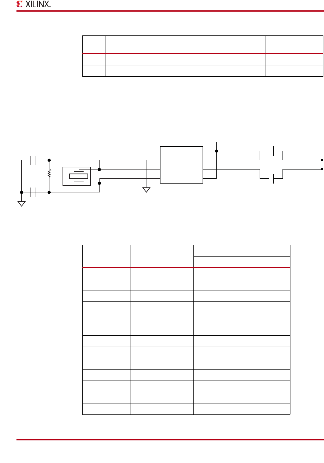
SGMII GTX Transceiver Clock Generation
An Integrated Circuit Systems ICS844021I chip generates a high-quality, low-jitter, 125-
MHz LVDS clock from an inexpensive 25-MHz crystal oscillator. This clock is sent to the
GTX driving the SGMII interface. Series AC coupling capacitors are also present to allow
the clock input of the FPGA to set the common mode voltage.
Table 1-13 shows the connections and pin numbers for the PHY.
CFG5 V
CC
2.5V DIS_FC = 1 DIS_SLEEP = 1 HWCFG_MD[3] = 1
CFG6 PHY_LED_RX SEL_BDT = 0 INT_POL = 1 75/50 OHM = 0
Table 1-12: Board Connections for PHY Configuration Pins (Cont’d)
Pin
Connection on
Board
Bit[2]
Definition and Value
Bit[1]
Definition and Value
Bit[0]
Definition and Value
X-Ref Target - Figure 1-13
Figure 1-13: Ethernet SGMII Clock - 125 MHz
VDDA_SGMIICLK
ICS84402II
VDDA VDD
VDD_SGMIICLK
SGMIICLK_QO_C_P
SGMIICLK_QO_P
SGMIICLK_QO_N
SGMIICLK_QO_C_N
Q0
NQ0
OE
GND
XTAL_OUT
XTAL_IN
1
2
3
4
U82
125.00 MHz Clock
GND_SGMIICLK
SGMIICLK_XTAL_OUT
SGMIICLK_XTAL_IN
8
7
6
5
X3
25.000MHZ
R132
DNP
1%
1/16W
C55 1
0.1UF
10V 2
X5R
C347
33PF
50V
NPO
C56 1
0.1UF
10V 2
X5R
1
2
C348
33PF
50V
NPO
1
2
1
2
UG534_13_111709
Table 1-13: Ethernet PHYConnections
U1 FPGA Pin Schematic Net Name
U80 M88E1111
Pin Number Pin Name
AN14 PHY_MDIO 33 MDIO
AP14 PHY_MDC 35 MDC
AH14 PHY_INT 32 INT_B
AH13 PHY_RESET 36 RESET_B
AL13 PHY_CRS 115 CRS
AK13 PHY_COL 114 COL
AP11 PHY_RXCLK 7 RXCLK
AG12 PHY_RXER 8 RXER
AM13 PHY_RXCTL_RXDV 4 RXDV
AN13 PHY_RXD0 3 RXD0
AF14 PHY_RXD1 128 RXD1
AE14 PHY_RXD2 126 RXD2
AN12 PHY_RXD3 125 RXD3


