72 www.xilinx.com ML605 Hardware User Guide
UG534 (v1.2.1) January 21, 2010
Chapter 1: ML605 Evaluation Board
FPGA Power Supply Margining
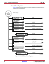
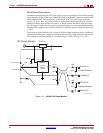
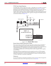
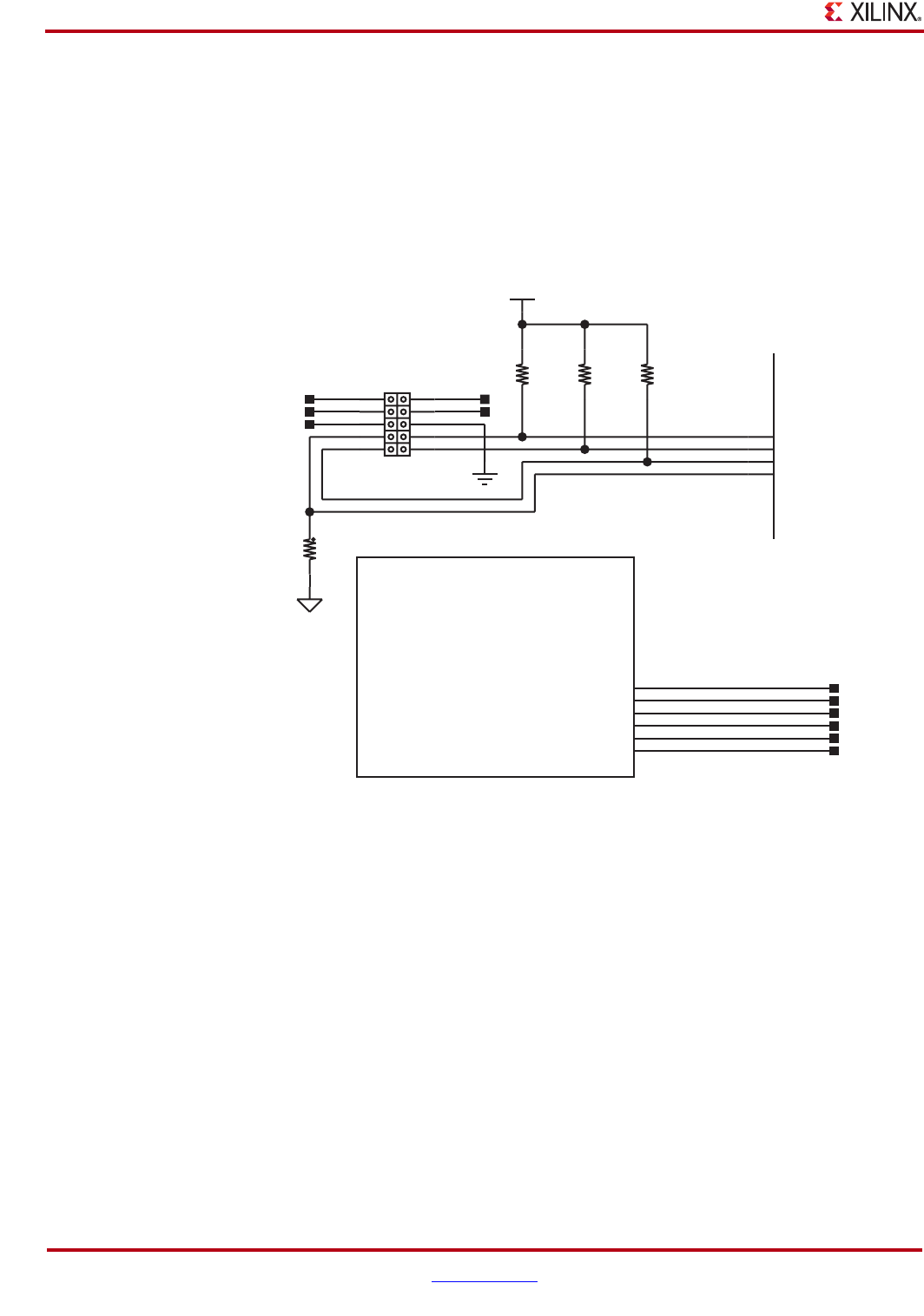
The PMBus (IIC), which provides access to the 2 x UDC9240 power controllers, can also be
accessed via FPGA I/O in addition to a dedicated header (J3), see Figure 1-33. A full
description of the UDC9240 functionality is outside the scope of this user guide. However,
this useful feature can be used, for example, to margin the FPGA and board power
supplies when evaluating a design. The System Monitor provides accurate measurements
of the on-chip supply voltages as the FPGA supplies are margined. The PMBus (and fan)
connections are shown in Figure 1-33.
System Monitor ML605 Demonstration Design
The various features described in this section are easily evaluated using a MicroBlaze™
based reference designed provided with the ML605 Evaluation Board. This reference
design supports a UART based interface using a terminal program such as Hyperterminal
to provide information on the FPGA power supplies, temperature, and power
consumption. In addition, the UART interface can be used to margin the FPGA supplies
over the PMBus.
The System Monitor functionality can also be accessed at any time via JTAG using the
ChipScope Pro Analyzer tool without design modifications or cores inserted into a user
design. The ChipScope Pro Analyzer tool automatically connects to the System Monitor
via a JTAG cable after a connection is established.
References
For more information on using the System Monitor and an overview of the tool support for
this feature, see the
Virtex-6 FPGA System Monitor User Guide. [Ref 15]
X-Ref Target - Figure 1-33
Figure 1-33: UDC9240 PMBus Access
9240
DGND1
AGND1
PMBus Connector
35
19
36
209
7
12
3
56
4
8
10
J3
PMBUS_DATA
PMBUS_ALERT
R301
100K
5% 5%
100K
R299 R300
100K
5%
PMBUS_CLK
PMBUS_CTRL
R335
1.0M
5%
TI_V3P3
UDC9240
NC
NC
NC
NC NC
IO_L9P_MRCC_34_L10
IO_L9N_MRCC_34_M10
IO_L10P_MRCC_34_AC10
IO_L10N_MRCC_34_AB10
IO_L11P_SRCC_34_AH9
IO_L11N_SRCC_34_AJ9
6vlx240tff1156
BANK 34
L10
M10
AC10
AB10
AH9
AJ9 PMBUS_CTRL_LS
SM_FAN_PWM
SM_FAN_TACH
PMBUS_ALERT_LS
PMBUS_CLK_LS
PMBUS_DATA_LS
UG534_35_081209


