


U2761A User’s Guide XV
List of Figures
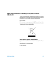
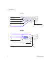
Figure 1-1 55-pin backplane connector pin configuration 23
Figure 2-1 U2761A soft front panel 28
Figure 2-2 Top panel view of the U2761A 29
Figure 2-3 Panel view of the frequency section 30
Figure 2-4 Panel view of the amplitude section 32
Figure 2-5 Panel view of the DC offset section 34
Figure 2-6 Panel view of the Tools menu 37
Figure 2-7 Square wave duty cycles 38
Figure 2-8 Panel view of the duty cycle section 39
Figure 2-9 Ramp wave duty cycles 40
Figure 2-10 Panel view of the symmetry section 40
Figure 2-11 Panel view of the output section 41
Figure 2-12 Pulse waveform 45
Figure 2-13 Panel view of the pulse width section 46
Figure 2-14 AM waveform 49
Figure 2-15 Panel view of AM 50
Figure 2-16 Panel view of the Arbitrary waveform 51
Figure 2-17 FM waveform 55
Figure 2-18 Panel view of FM 56
Figure 2-19 PM waveform 61
Figure 2-20 Panel view of PM 62
Figure 2-21 FSK modulation waveform 66
Figure 2-22 Panel view of FSK 67
Figure 2-23 PSK modulation waveform 71
Figure 2-24 Panel view of PSK 72
Figure 2-25 ASK modulation waveform 76
Figure 2-26 Panel view of ASK 77
Figure 2-27 Frequency sweep 80
Figure 2-28 Panel view of sweep 81
Figure 2-29 Trigger input pulse 88