


II-12
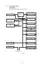
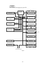
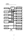
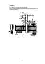
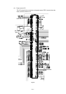
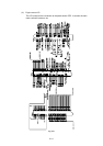
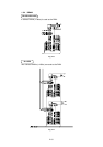
The ASIC is composed of a Cell Based IC that contains the following functional blocks.
(1) Oscillator circuit
Generates the main clock for the CPU.
(2) Address decoder
Generates the CS for each device.
(3) DRAM control
Generates the RAS, CAS, WE, OE and MA signals for the DRAM and controls
refresh processing (CAS before RAS self-refreshing method).
(4) Interrupt control
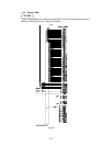
Interrupt levels:
Priority High 10 Reserve interrupt 1 (for debug)
9 Watch Dog Timer
8 LSB EMPTY (for VDO FIFO)
7 Timer 1
6 USB
5 XIO interrupt (RS-100M) or MIO interrupt
4 BD (for engine check)
3 Reserve interrupt 2
2 CDCC
Low 1 Timer 2
Note:
All the interrupts can be masked.
The priority of levels 7, 6, and 5 are changeable from the program.
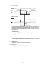
(5) Timers
The following timers are incorporated:
Timer 1 32-bit timer
Timer 2 32-bit timer
Timer 3 Watch-dog timer
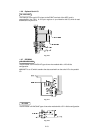
(6) FIFO
A 10Kbit FIFO is included. Data for one raster scan is transferred from the RAM to
the FIFO by DMA transmission and is output as serial video data. The data cycle is
10.43MHz.
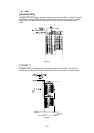
(7) Parallel I/O
<Data receive Mode>
There are two modes in this unit. One is the CPU receive mode and the other is
the DMA receive mode. In the CPU receive mode the CPU receives the command
data from the PC, and after the CPU is switched to the DMA mode, it receives the
image data and writes it to the DRAM directly.
HL-1050