CY7C67300
Document #: 38-08015 Rev. *J Page 14 of 99
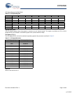
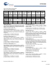
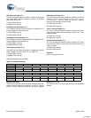
External (Remote) Wakeup Source
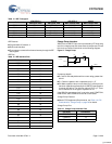
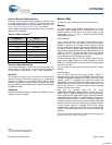
There are several possible events available to wake EZ-Host
from Sleep mode as shown in Table 20. These may also be used
as remote wakeup options for USB applications. See the Power
Control Register [0xC00A] [R/W] on page 19 for details.
Upon wakeup, code begins executing within 200 µs, the time it
takes the PLL to stabilize.
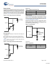
Power-On-Reset Description
The length of the power-on-reset event can be defined by (V
CC
ramp to valid) + (Crystal startup). A typical application might use
a 12 ms power-on-reset event = ~7 ms + ~5 ms, respectively.
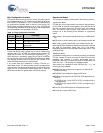
Reset Pin
The Reset pin is active low and requires a minimum pulse
duration of sixteen 12 MHz clock cycles (1.3 µs). A reset event
restores all registers to their default POR settings. Code
execution then begins 200 µs later at 0xFF00 with an immediate
jump to 0xE000, the start of BIOS. Refer to BIOS documentation
for additional details.
USB Reset
A USB Reset affects registers 0xC090 and 0xC0B0, all other
registers remain unchanged.
Memory Map
The memory map is discussed in the following sections.
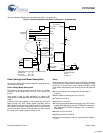
Mapping
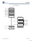
The total memory space directly addressable by the CY16
processor is 64K (0x0000-0xFFFF). Program, data, and IO are
contained within this 64K space. This memory space is byte
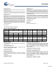
addressable. Figure 10 on page 15 shows the various memory
region address locations.
Internal Memory
Of the internal memory, 15K bytes are allocated for user's
program and data. The lower memory space from 0x0000 to
0x04A2 is reserved for interrupt vectors, general purpose
registers, USB control registers, stack, and other BIOS variables.
The upper internal memory space contains EZ-Host control
registers from 0xC000 to 0xC0FF and the BIOS ROM itself from
0xE000 to 0xFFFF. For more information about the reserved
lower memory or the BIOS ROM, refer to the Programmer’s
documentation and/or the BIOS documentation.
During development with the EZ-Host toolset, leave the lower
area of user's space (0x04A4 to 0x1000) available to load the
GDB stub. The GDB stub is required to allow the toolset debug
access into EZ-Host.
The chip select pins are not active during accesses to internal
memory.
External Memory
Up to 32 KB of external memory from 0x4000 - 0xBFFF is
available via one chip select line (nXRAMSEL) with RAM Merge
enabled (BIOS default). Additionally, another 8 KB region from
0xC100 - 0xDFFF is available via a second chip select line
(nXROMSEL) giving 40 KB of total available external memory.
Together with the internal 15 KB, this gives a total of either ~48
KB (one chip select) or ~56 KB (two chip selects) of available
memory for either code or data.
Note that the memory map and pin names
(nXRAMSEL/nXROMSEL) define specific memory regions for
RAM vs. ROM. This allows the BIOS to look in the upper external
memory space at 0xC100 for SCAN vectors (enabling code to be
loaded/executed from ROM). If no SCAN vectors are required in
the design (external memory is used exclusively for data), then
all external memory regions can be used for RAM. Similarly, the
external memory can be used exclusively for code space (ROM).
If more external memory is required, EZ-Host has enough
address lines to support up to 512 KB. However, this requires
complex code banking/paging schemes via the Extended Page
registers.
For further information about setting up the external memory, see
the External Memory Interface on page 5.
Table 20. Wakeup Sources
[5, 6]
Wakeup Source
(if enabled)
Event
USB Resume D+/D– Signaling
OTGVBUS Level
OTGID Any Edge
HPI Read
HSS Read
SPI Read
IRQ1 (GPIO 25) Any Edge
IRQ0 (GPIO 24) Any Edge
Notes
5. Read data is discarded (dummy data).
6. HPI_INT asserts on a USB Resume.
[+] Feedback


