CY7C67300
Document #: 38-08015 Rev. *J Page 72 of 99
SPI Transmit Count Register [0xC0DA] [R/W]
Register Description
The SPI Transmit Count register designates the block byte
length for the SPI transmit DMA transfer.
Count (Bits [10:0])
The Count field sets the count for the SPI transmit DMA transfer.
Reserved
Write all reserved bits with ’0’.
SPI Receive Address Register [0xC0DC [R/W]
Register Description
The SPI Receive Address register is issued as the base address
for the SPI Receive DMA.
Address (Bits [15:0])
The Address field sets the base address for the SPI receive
DMA.
SPI Receive Count Register [0xC0DE] [R/W]
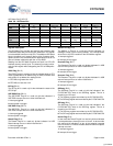
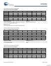
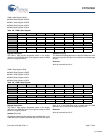
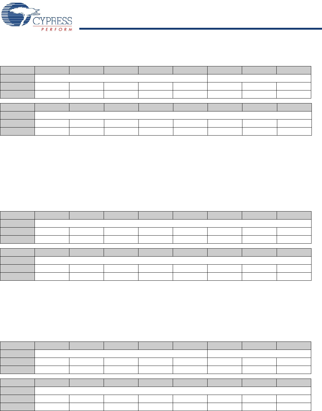
Table 116. SPI Transmit Count Register
Bit # 15 14 13 12 11 10 9 8
Field Reserved Count...
Read/Write - - - - - R/W R/W R/W
Default 0 0 0 0 0 0 0 0
Bit # 7 6 5 4 3 2 1 0
Field ...Count
Read/Write R/W R/W R/W R/W R/W R/W R/W R/W
Default 0 0 0 0 0 0 0 0
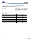
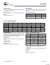
Table 117. SPI Receive Address Register
Bit # 15 14 13 12 11 10 9 8
Field Address...
Read/Write R/W R/W R/W R/W R/W R/W R/W R/W
Default 0 0 0 0 0 0 0 0
Bit # 7 6 5 4 3 2 1 0
Field ...Address
Read/Write R/W R/W R/W R/W R/W R/W R/W R/W
Default 0 0 0 0 0 0 0 0
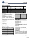
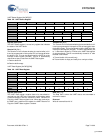
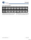
Table 118. SPI Receive Count Register
Bit # 15 14 13 12 11 10 9 8
Field Reserved Count...
Read/Write - - - - - R/W R/W R/W
Default 0 0 0 0 0 0 0 0
Bit # 7 6 5 4 3 2 1 0
Field ...Count
Read/Write R/W R/W R/W R/W R/W R/W R/W R/W
Default 0 0 0 0 0 0 0 0
[+] Feedback


