CY7C67300
Document #: 38-08015 Rev. *J Page 71 of 99
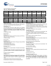
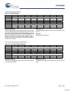
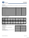
SPI Data Register [0xC0D6] [R/W]
Register Description
The SPI Data register contains data received on the SPI port
when read. Reading it empties the eight byte receive FIFO in PIO
byte mode. This receive data is valid when the Receive Interrupt
Bit of the SPI Status register is set to ‘1’ (RxIntVal triggers) or the
Receive Data Ready bit of the SPI Control register is set to ‘1’.
Writing to this register in PIO byte mode initiates a transfer of
data, the number of bits defined by Transmit Bit Length field in
the SPI Control register.
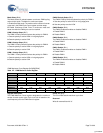
Data (Bits [7:0])
The Data field contains data received or to be transmitted on the
SPI port.
Reserved
Write all reserved bits with ’0’.
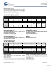
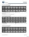
SPI Transmit Address Register [0xC0D8] [R/W]
Register Description
The SPI Transmit Address register is used as the base address
for the SPI transmit DMA.
Address (Bits [15:0])
The Address field sets the base address for the SPI transmit
DMA.
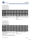
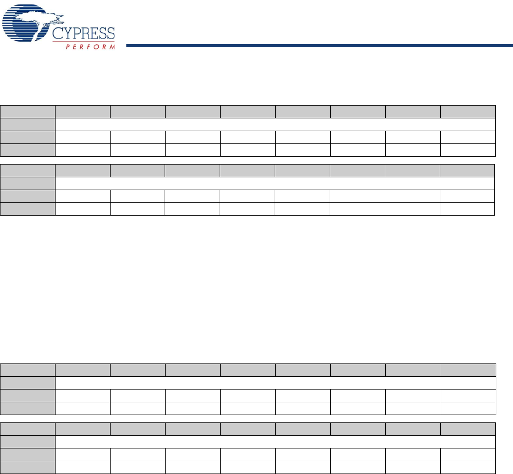
Table 114. SPI Data Register
Bit # 15 14 13 12 11 10 9 8
Field Reserved
Read/Write - - - - - - - -
Default X X X X X X X X
Bit # 7 6 5 4 3 2 1 0
Field Data
Read/Write R/W R/W R/W R/W R/W R/W R/W R/W
Default X X X X X X X X
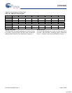
Table 115. SPI Transmit Address Register
Bit # 15 14 13 12 11 10 9 8
Field Address...
Read/Write R/W R/W R/W R/W R/W R/W R/W R/W
Default 0 0 0 0 0 0 0 0
Bit # 7 6 5 4 3 2 1 0
Field ...Address
Read/Write R/W R/W R/W R/W R/W R/W R/W R/W
Default 0 0 0 0 0 0 0 0
[+] Feedback


