CY7C67300
Document #: 38-08015 Rev. *J Page 91 of 99
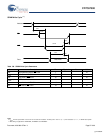
IDE Timing
The IDE interface supports PIO mode 0-4 as specified in the Information Technology-AT Attachment–4 with Packet Interface Extension
(ATA/ATAPI-4) Specification, T13/1153D Rev 18.
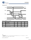
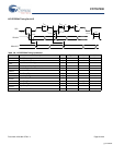
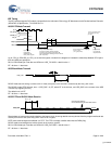
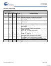
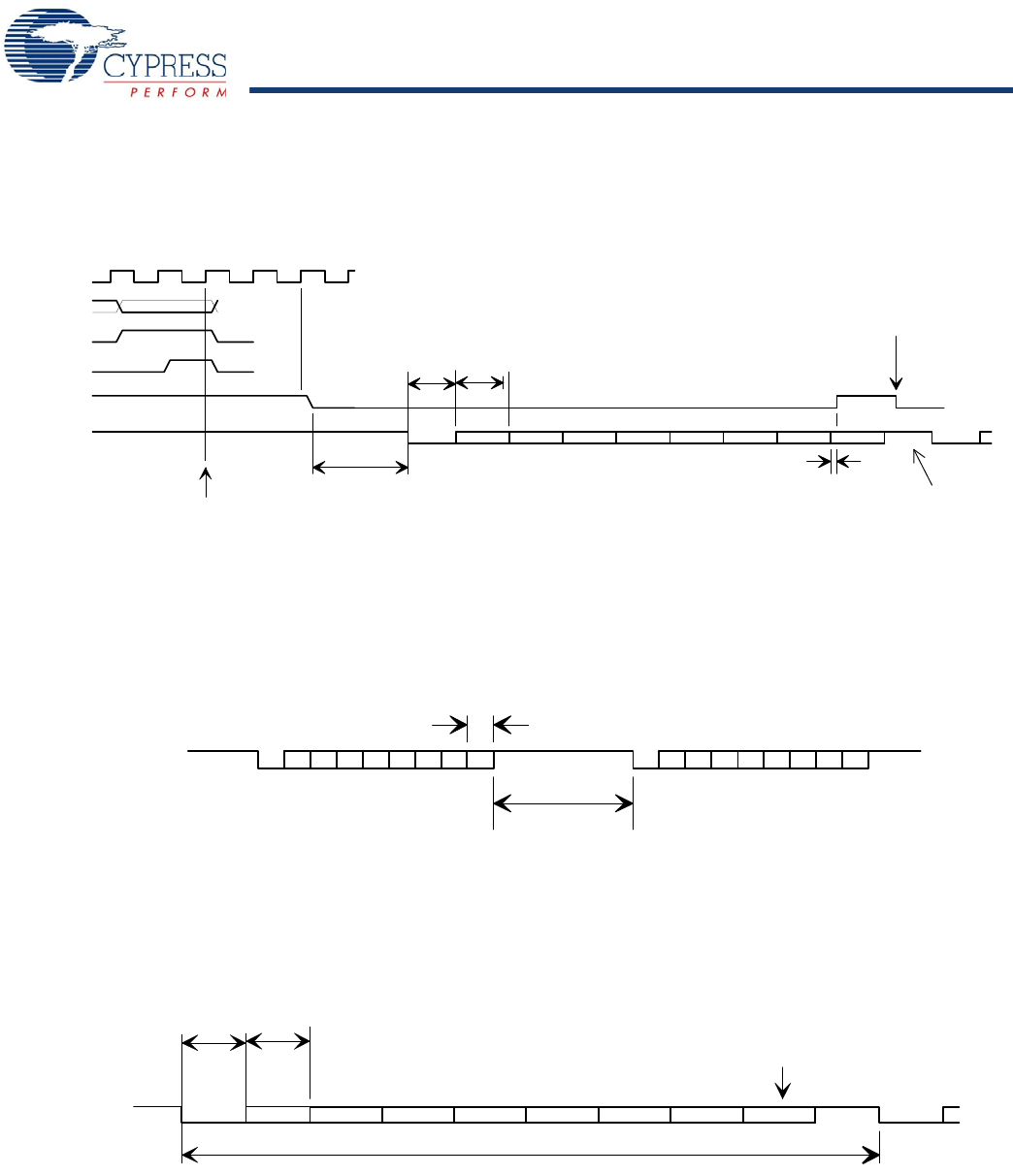
HSS BYTE Mode Transmit
qt_clk, CPU_A, CPUHSS_cs, CPU_wr are internal signals, included in the diagram to illustrate the relationship between CPU opera-
tions and HSS port operations.
Bit 0 is LSB of data byte. Data bits are HIGH true: HSS_TxD HIGH = data bit value ‘1’.
BT = bit time = 1/baud rate.
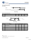
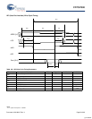
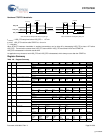
HSS Block Mode Transmit
BLOCK mode transmit timing is similar to BYTE mode, except the STOP bit time is controlled by the HSS_GAP value.
The BLOCK mode STOP bit time, t
GAP
= (HSS_GAP – 9) BT, where BT is the bit time, and HSS_GAP is the content of the HSS
Transmit Gap register [0xC074].
The default t
GAP
is 2 BT.
BT = bit time = 1/baud rate.
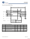
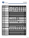
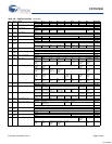
HSS BYTE and BLOCK Mode Receive
Receive data arrives asynchronously relative to the internal clock. Incoming data bit rate may deviate from the programmed baud rate
clock by as much as ±5% (with HSS_RATE value of 23 or higher).
BYTE mode received bytes are buffered in a FIFO. The FIFO not empty condition becomes the RxRdy flag.
BLOCK mode received bytes are written directly to the memory system.
Bit 0 is LSB of data byte. Data bits are HIGH true: HSS_RxD HIGH = data bit value ‘1’.
BT = bit time = 1/baud rate.
CPU may start another BYTE
transmit right after TxRdy
goes high
start of last data bit to TxRdy high:
0 min, 4 T max.
(T is qt_clk period)
TxRdy low to start bit delay:
0 min, BT max when starting from IDEL.
For back to back transmit, new START Bit
begins immediately following previous STOP bit.
(BT = bit period)
BT
BT
start bit bit 0
bit 1 bit 2 bit 3 bit 4 bit 5 bit 6 bit 7
qt_clk
CPU_A[2:0]
CPUHSS_cs
CPU_wr
TxRdy flag
HSS_TxD
Byte transmit
triggered by a
CPU write to the
HSS_TxData register
stop bit start bit
programmable
1 or 2 stop bits.
1 stop bit shown.
HSS_TxD
t
GAP
BT
BT +/- 5%
start bit bit 0
bit 1 bit 2 bit 3 bit 4 bit 5 bit 6 bit 7 stop bit start bit
HSS_RxD
BT +/- 5%
10 BT +/- 5%
received byte added to
receive FIFO during the final data bit time
[+] Feedback


