CY7C67300
Document #: 38-08015 Rev. *J Page 25 of 99
External Memory Control Register [0xC03A] [R/W]
Register Description
The External Memory Control register provides control of Wait
States for the external SRAM or ROM. All wait states are based
off of 48 MHz.
XRAM Merge Enable (Bit 13)
The XRAM Merge Enable bit enables or disables the RAM merge
feature. When the RAM merge feature is enabled, the
nXRAMSEL is active whenever the nXMEMSEL is active.
1: Enable RAM merge
0: Disable RAM merge
XROM Merge Enable (Bit 12)
The XROM Merge Enable bit enables or disables the ROM
merge feature. When the ROM merge feature is enabled, the
nXROMSEL is active whenever the nXMEMSEL is active.
1: Enable ROM merge
0: Disable ROM merge
XMEM Width Select (Bit 11)
The XMEM Width Select bit selects the extended memory width.
1: Extended memory = 8
0: Extended memory = 16
XMEM Wait Select (Bits [10:8])
The XMEM Wait Select field selects the extended memory wait
state from 0 to 7.
XROM Width Select (Bit 7)
The XROM Width Select bit selects the external ROM width.
1: External memory = 8
0: External memory = 16
XROM Wait Select (Bits[6:4])
The XROM Wait Select field selects the external ROM wait state
from 0 to 7.
XRAM Width Select (Bit 3)
The XRAM Width Select bit selects the external RAM width.
1: External memory = 8
0: External memory = 16
XRAM Wait Select (Bits[2:0])
The XRAM Wait Select field selects the external RAM wait state
from 0 to 7.
Reserved
Write all reserved bits with ’0’.
Timer Registers
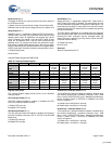
There are three registers dedicated to timer operations. Each of
these registers are discussed in this section and are summarized
in Table 39.
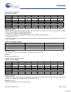
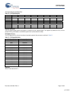
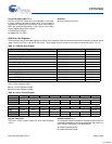
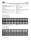
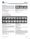
Table 38. External Memory Control Register
Bit # 15 14 13 12 11 10 9 8
Field
Reserved XRAM Merge
Enable
XROM Merge
Enable
XMEM Width
Select
XMEM Wait
Select
Read/Write - - R/W R/W R/W R/W R/W R/W
Default X X X X X X X X
Bit # 7 6 5 4 3 2 1 0
Field
XROM Width
Select
XROM Wait
Select
XRAM Width
Select
XRAM Wait
Select
Read/Write R/W R/W R/W R/W R/W R/W R/W R/W
Default X X X X X X X X
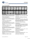
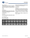
Table 39. Timer Registers
Register Name Address R/W
Watchdog Timer Register 0xC00C R/W
Timer 0 Register 0xC010 R/W
Timer 1 Register 0xC012 R/W
[+] Feedback


